8Kx8 Static RAM
CY7C186
Cypress Semiconductor Corporation
∑
3901 North First Street
∑
San Jose
∑
CA 95134
∑
408-943-2600
Document #: 38-05280 Rev. **
Revised March 22, 2002
86
Features
∑ High speed
-- 20 ns
∑ Low active power
-- 605 mW
∑ Low standby power
-- 110 mW
∑ CMOS for optimum speed/power
∑ Easy memory expansion with CE
1
, CE
2
, and OE
features
∑ TTL-compatible inputs and outputs
∑ Automatic power-down when deselected
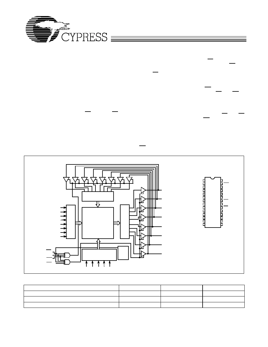
Functional Description
The CY7C186 is a high-performance CMOS static RAM orga-
nized as 8192 words by 8 bits. Easy memory expansion is
provided by an active LOW chip enable (CE
1
), an active HIGH
chip enable (CE
2
), and active LOW output enable (OE) and
three-state drivers. The device has an automatic power-down
feature (CE
1
), reducing the power consumption by over 80%
when deselected. The CY7C186 is in a 600-mil-wide PDIP
package and a 32-pin TSOP (std. pinout).
An active LOW write enable signal (WE) controls the writ-
ing/reading operation of the memory. When CE
1
and WE in-
puts are both LOW and CE
2
is HIGH, data on the eight data
input/output pins (I/O
0
through I/O
7
) is written into the memory
location addressed by the address present on the address
pins (A0 through A12). Reading the device is accomplished by
selecting the device and enabling the outputs, CE
1
and OE
active LOW, CE
2
active HIGH, while WE remains inactive or
HIGH. Under these conditions, the contents of the location ad-
dressed by the information on address pins are present on the
eight data input/output pins.
The input/output pins remain in a high-impedance state unless
the chip is selected, outputs are enabled, and write enable
(WE) is HIGH. A die coat is used to insure alpha immunity.
LogicBlock Diagram
Pin Configuration
A
1
A
2
A
3
A
4
A
5
A
6
A
7
A
8
A
0
A
10
A
9
A
11
A
12
I/O
0
1
2
3
4
5
6
7
8
9
10
11
12
13
14
28
27
26
25
24
23
22
21
20
19
18
17
16
15
V
CC
WE
CE
2
A
3
A
2
A
1
OE
A
0
CE
1
I/O
7
I/O
6
I/O
5
I/O
4
I/O
3
NC
A
4
A
5
A
6
A
7
A
8
A
9
A
10
A
11
A
12
I/O
0
I/O
1
I/O
2
GND
256 x 32 x 8
ARRAY
INPUT BUFFER
COLUMN DECODER
ROW
D
E
CODE
R
S
E
N
S
E AM
PS
POWER
DOWN
I/O
1
I/O
2
I/O
3
I/O
4
I/O
5
I/O
6
I/O
7
CE
1
CE
2
WE
OE
Top View
DIP
Selection Guide
[1]
7C186-20
7C186-25
7C186-35
Maximum Access Time (ns)
20
25
35
Maximum Operating Current (mA)
110
100
100
Maximum Standby Current (mA)
20/15
20/15
20/15
Notes:
1.
For military specifications, see the CY7C186A datasheet.
CY7C186
Document #: 38-05280 Rev. **
Page 2 of 9
Maximum Ratings
(Above which the useful life may be impaired. For user guide-
lines, not tested.)
Storage Temperature ................................. ≠65
∞
C to +150
∞
C
Ambient Temperature with
Power Applied............................................. ≠55
∞
C to +125
∞
C
Supply Voltage to Ground Potential ............... ≠0.5V to +7.0V
DC Voltage Applied to Outputs
in High Z State
[2]
............................................ ≠0.5V to +7.0V
DC Input Voltage
[2]
........................................ ≠0.5V to +7.0V
Output Current into Outputs (LOW)............................. 20 mA
Static Discharge Voltage .......................................... >2001V
(per MIL-STD-883, Method 3015)
Latch-Up Current .................................................... >200 mA
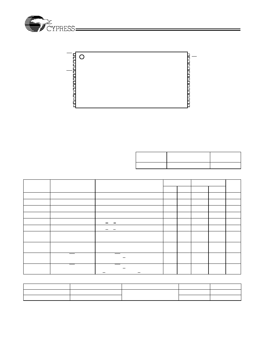
Pin Configurations
(continued)
1
2
3
4
5
6
7
8
9
10
11
14
19
20
24
23
22
21
25
28
27
26
Top View
TSOP
12
13
29
32
21
30
OE
A
1
A
2
A
3
CE
2
WE
V
CC
NC
NC
A
4
A
5
A
6
A
7
A
0
CE
I/O
7
I/O
6
I/O
5
I/O
4
I/O
3
NC
NC
GND
I/O
2
I/O
1
I/O
0
A
12
C186-3
NC
16
17
18
15
A
8
A
9
A
11
A
10
Operating Range
Range
Ambient
Temperature
V
CC
Commercial
0
∞
C to +70
∞
C
5V
±
10%
Electrical Characteristics
Over the Operating Range
Parameter
Description
Test Conditions
7C186-20
7C186-25,35
Unit
Min.
Max.
Min.
Max.
V
OH
Output HIGH Voltage
V
CC
= Min., I
OH
= ≠4.0 mA
2.4
2.4
V
V
OL
Output LOW Voltage
V
CC
= Min., I
OL
= 8.0 mA
0.4
0.4
V
V
IH
Input HIGH Voltage
2.2
V
CC
2.2
V
CC
V
V
IL
Input LOW Voltage
[2]
≠0.5
0.8
≠0.5
0.8
V
I
IX
Input Load Current
GND < V
I
< V
CC
≠5
+5
≠5
+5
µ
A
I
OZ
Output Leakage Current GND < V
I
< V
CC
, Output Disabled
≠5
+5
≠5
+5
µ
A
I
OS
Output Short
Circuit Current
[3]
V
CC
= Max.,
V
OUT
= GND
≠300
≠300
mA
I
CC
V
CC
Operating
Supply Current
V
CC
= Max.,
I
OUT
= 0 mA
110
100
mA
I
SB1
Automatic CE
1
Power-Down Current
Max. V
CC
, CE
1
> V
IH,
Min. Duty Cycle=100%
20
20
mA
I
SB2
Automatic CE
1
Power-Down Current
Max. V
CC
, CE
1
> V
CC
≠ 0.3V,
V
IN
> V
CC
≠ 0.3V or V
IN
< 0.3V
15
15
mA
Capacitance
[4]
Parameter
Description
Test Conditions
Max.
Unit
C
IN
Input Capacitance
T
A
= 25
∞
C, f = 1 MHz,
V
CC
= 5.0V
7
pF
C
OUT
Output Capacitance
7
pF
Notes:
2.
Minimum voltage is equal to
≠
3.0V for pulse durations less than 30 ns.
3.
Not more than 1 output should be shorted at one time. Duration of the short circuit should not exceed 30 seconds.
4.
Tested initially and after any design or process changes that may affect these parameters.
CY7C186
Document #: 38-05280 Rev. **
Page 3 of 9
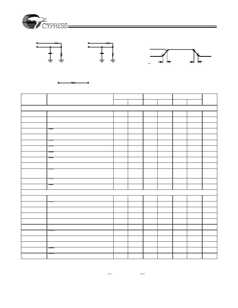
AC Test Loads and Waveforms
R1 481
3.0V
5V
OUTPUT
R1 481
R2
255
30 pF
GND
90%
90%
10%
5 ns
5 ns
5V
OUTPUT
R2
255
5 pF
(a)
(b)
OUTPUT
1.73V
INCLUDING
JIG AND
SCOPE
INCLUDING
JIG AND
SCOPE
10%
Equivalent to:
TH …VENIN EQUIVALENT
ALL INPUT PULSES
167
Switching Characteristics
Over the Operating Range
[5]
7C186-20
7C186-25
7C186-35
Parameter
Description
Min.
Max.
Min.
Max.
Min.
Max.
Unit
READ CYCLE
t
RC
Read Cycle Time
20
25
35
ns
t
AA
Address to Data Valid
20
25
35
ns
t
OHA
Data Hold from Address Change
5
5
5
ns
t
ACE1
CE
1
LOW to Data Valid
20
25
35
ns
t
ACE2
CE
2
HIGH to Data Valid
20
25
35
ns
t
DOE
OE LOW to Data Valid
9
12
15
ns
t
LZOE
OE LOW to Low Z
3
3
3
ns
t
HZOE
OE HIGH to High Z
[6]
8
10
10
ns
t
LZCE1
CE
1
LOW to Low Z
[7]
5
5
5
ns
t
LZCE2
CE
2
HIGH to Low Z
3
3
3
ns
t
HZCE
CE
1
HIGH to High Z
[6, 7]
CE
2
LOW to High Z
8
10
10
ns
t
PU
CE
1
LOW to Power-Up
0
0
0
ns
t
PD
CE
1
HIGH to Power-Down
20
20
20
ns
WRITE CYCLE
[8]
t
WC
Write Cycle Time
20
25
35
ns
t
SCE1
CE
1
LOW to Write End
15
20
20
ns
t
SCE2
CE
2
HIGH to Write End
15
20
20
ns
t
AW
Address Set-Up to Write End
15
20
25
ns
t
HA
Address Hold from Write End
0
0
0
ns
t
SA
Address Set-Up to Write Start
0
0
0
ns
t
PWE
WE Pulse Width
15
15
20
ns
t
SD
Data Set-Up to Write End
10
10
12
ns
t
HD
Data Hold from Write End
0
0
0
ns
t
HZWE
WE LOW to High Z
[6]
7
7
8
ns
t
LZWE
WE HIGH to Low Z
5
5
5
ns
Notes:
5.
Test conditions assume signal transition time of 5 ns or less, timing reference levels of 1.5V, input pulse levels of 0 to 3.0V, and output loading of the specified
I
OL
/I
OH
and 30-pF load capacitance.
6.
t
HZOE,
t
HZCE
, and t
HZWE
are specified with C
L
= 5 pF as in part (b) of AC Test Loads. Transition is measured
±
500 mV from steady-state voltage.
7.
At any given temperature and voltage condition, t
HZCE
is less than t
LZCE
for any given device.
8.
The internal write time of the memory is defined by the overlap of CE
1
LOW, CE
2
HIGH, and WE LOW. All signals must be active to initiate a write, and any
signal can terminate a write by going inactive. The data input set-up and hold timing should be referenced to the trailing edge of the signal that terminates the
write.
CY7C186
Document #: 38-05280 Rev. **
Page 4 of 9
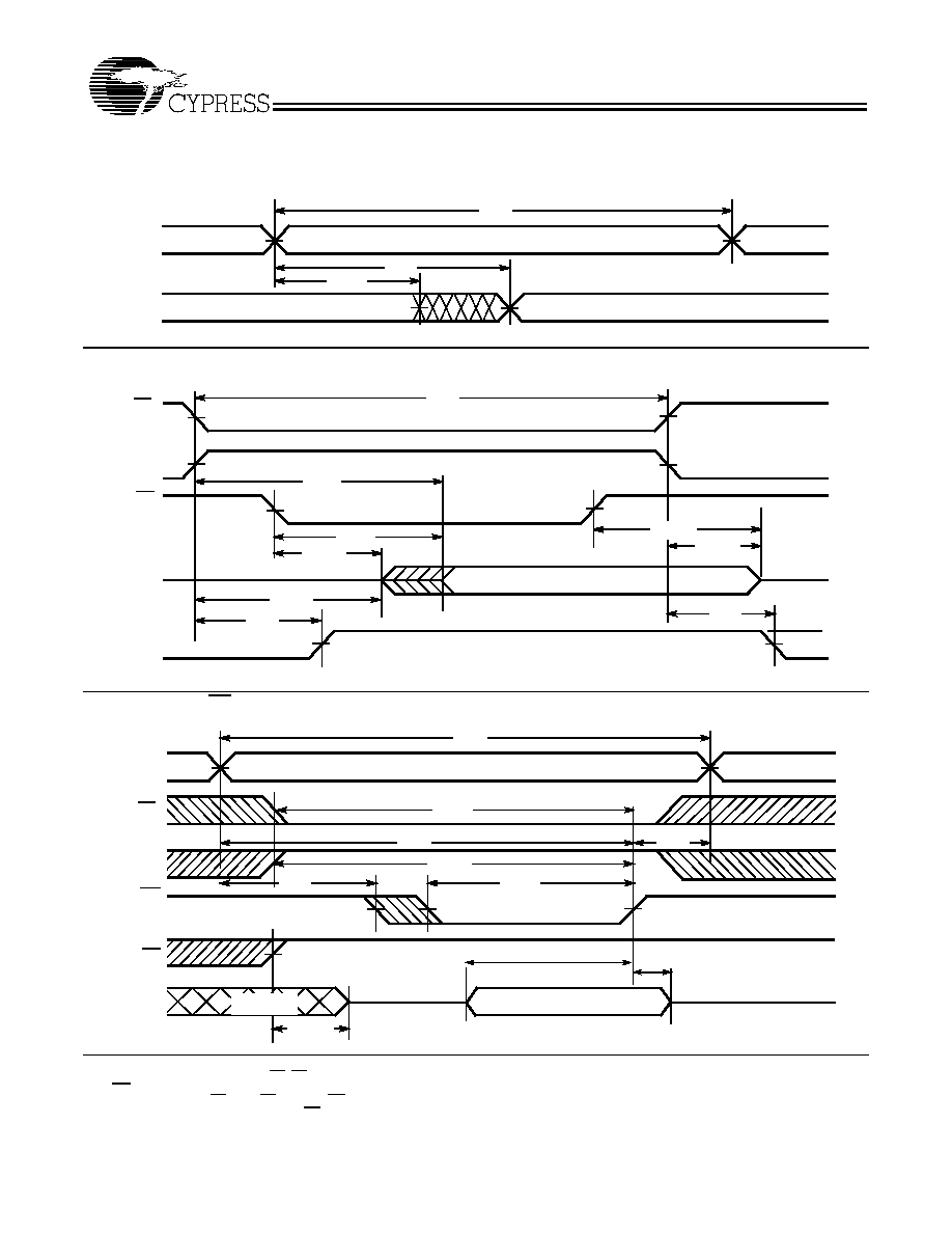
Switching Waveforms
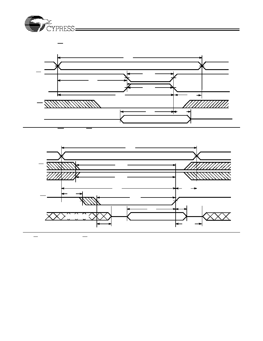
Read Cycle No. 1
[9]
Read Cycle No. 2
[10, 11]
Write Cycle No. 1 (WE Controlled)
[11, 12]
Notes:
9.
Device is continuously selected. OE, CE
1
= V
IL
. CE
2
= V
IH.
10. WE is HIGH for read cycle.
11.
Data I/O is High Z if OE = V
IH
, CE
1
= V
IH
, or WE = V
IL
.
12. Address valid prior to or coincident with CE
1
transition LOW and CE
2
transition HIGH.
13. During this period, the I/Os are in the output state and input signals should not be applied.
ADDRESS
DATA OUT
PREVIOUS DATA VALID
DATA VALID
t
RC
t
AA
t
OHA
50%
50%
DATA VALID
t
RC
t
ACE
t
DOE
t
LZOE
t
LZCE
t
PU
HIGH IMPEDANCE
IMPEDANCE
ICC
ISB
t
HZOE
t
HZCE
t
PD
OE
HIGH
DATA OUT
V
CC
SUPPLY
CURRENT
CE
1
OE
CE
2
t
HD
t
SD
t
PWE
t
SA
t
HA
t
AW
t
WC
t
HZOE
DATA
IN
VALID
CE
CE
1
OE
WE
CE
2
DATA I/O
t
SCEI
t
SCE2
ADDRESS
NOTE 13
CY7C186
Document #: 38-05280 Rev. **
Page 5 of 9
Write Cycle No. 2 (CE Controlled)
[11,12,14]
Write Cycle No. 3 (WE Controlled, OE LOW)
[11, 14]
Notes:
14. If CE
1
goes HIGH simultaneously with WE HIGH, the output remains in a high-impedance state.
Switching Waveforms
(continued)
t
WC
t
AW
t
SA
t
HA
t
HD
t
SD
t
SCE1
WE
DATA I/O
ADDRESS
CE
1
DATA
IN
VALID
t
SCE2
CE
2
t
HD
tSD
t
LZWE
t
SA
t
HA
t
AW
t
WC
t
HZWE
DATA
IN
VALID
t
SCE1
t
SCE2
CE
1
CE
2
ADDRESS
DATA I/O
WE
NOTE 13
t
PWE