 | –≠–ª–µ–∫—Ç—Ä–æ–Ω–Ω—ã–π –∫–æ–º–ø–æ–Ω–µ–Ω—Ç: CY7C187A | –°–∫–∞—á–∞—Ç—å:  PDF PDF  ZIP ZIP |
64K x 1 Static RAM
CY7C187
Cypress Semiconductor Corporation
∑
3901 North First Street
∑
San Jose
∑
CA 95134
∑
408-943-2600
Document #: 38-05044 Rev. **
Revised August 24, 2001
87
Features
∑ High speed
-- 15 ns
∑ CMOS for optimum speed/power
∑ Low active power
-- 495 mW
∑ Low standby power
-- 220 mW
∑ TTL compatible inputs and outputs
∑ Automatic power-down when deselected
Functional Description
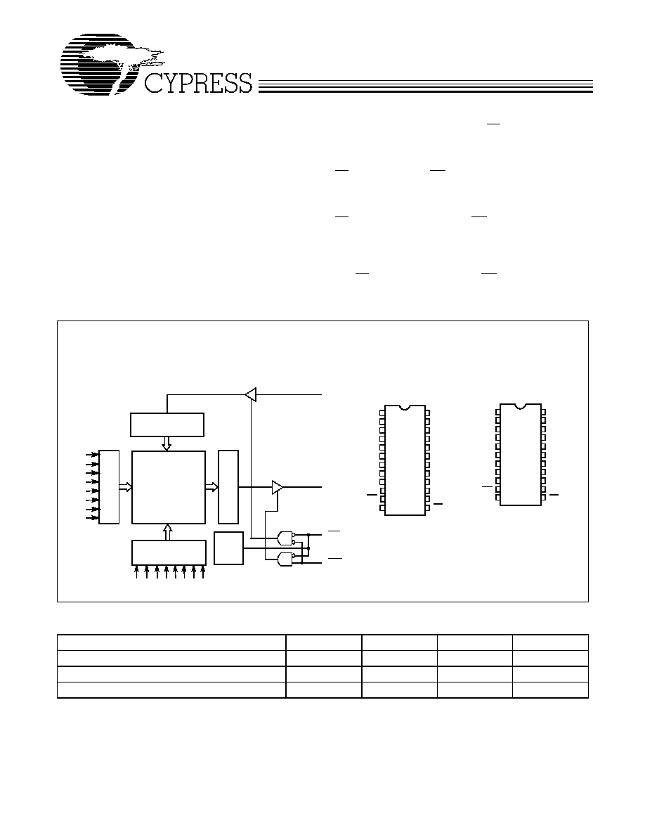
The CY7C187 is a high-performance CMOS static RAM orga-
nized as 65,536 words x 1 bit. Easy memory expansion is pro-
vided by an active LOW Chip Enable (CE) and three-state driv-
ers. The CY7C187 has an automatic power-down feature,
reducing the power consumption by 56% when deselected.
Writing to the device is accomplished when the Chip Enable
(CE) and Write Enable (WE) inputs are both LOW. Data on the
input pin (D
IN
) is written into the memory location specified on
the address pins (A
0
through A
15
).
Reading the device is accomplished by taking the Chip Enable
(CE) LOW, while Write Enable (WE) remains HIGH. Under
these conditions, the contents of the memory location speci-
fied on the address pin will appear on the data output (D
OUT
)
pin.
The output pin stays in high-impedance state when Chip En-
able (CE) is HIGH or Write Enable (WE) is LOW.
The CY7C187 utilizes a die coat to insure alpha immunity.
Logic Block Diagram
Pin Configurations
256 x 256
ARRAY
C187≠1
A
12
A
13
A
14
A
15
A
0
A
1
A
2
A
3
A
4
A
5
A
10
A
11
COLUMN DECODER
ROW
DE
CODE
R
S
E
N
S
E AM
PS
INPUT BUFFER
POWER
DOWN
DI
DO
CE
WE
A
7
A
6
A
9
A
8
1
2
3
4
5
6
7
8
9
10
11
12
13
14
18
17
16
15
19
22
21
20
Top View
DIP
A
0
A
1
A
2
A
3
A
4
D
OUT
WE
GND
CE
V
CC
A
15
A
14
A
13
A
12
A
10
A
9
A
8
D
IN
A
11
C187≠2
WE
1
2
3
4
5
6
7
8
9
10
11
14
15
16
20
19
18
17
21
24
23
22
Top View
SOJ
A
0
A
1
A
2
A
3
A
4
NC
CE
V
CC
A
15
A
14
A
13
A
12
A
10
A
9
A
8
D
IN
NC
GND
D
OUT
12
13
C187≠3
A
5
A
6
A
7
A
11
A
5
A
6
A
7
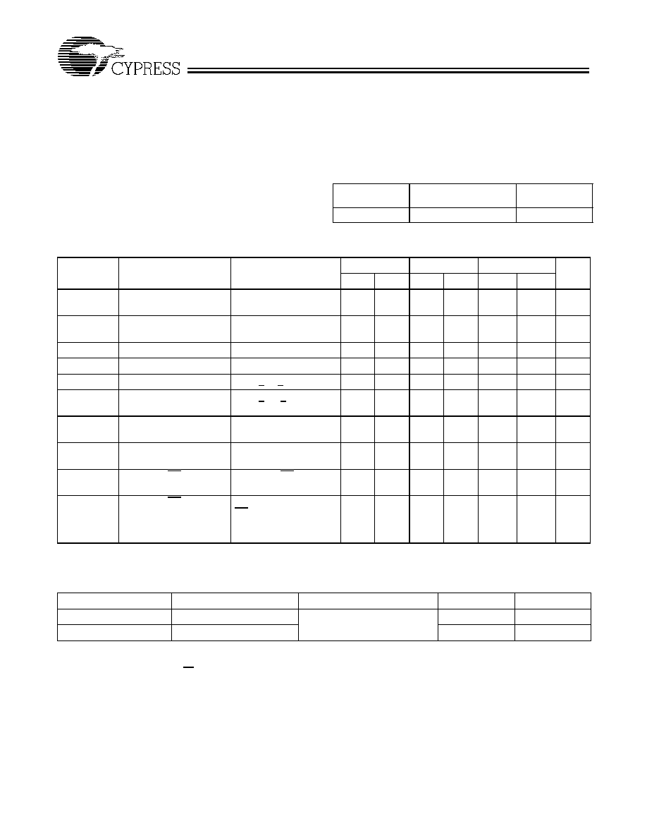
Selection Guide
[1]
7C187-15
7C187-20
7C187-25
7C187-35
Maximum Access Time (ns)
15
20
25
35
Maximum Operating Current (mA)
90
80
70
70
Maximum Standby Current (mA)
40/20
40/20
20/20
20/20
Note:
1.
For military specifications, see the CY7C187A datasheet.
CY7C187
Document #: 38-05044 Rev. **
Page 2 of 9
Maximum Ratings
(Above which the useful life may be impaired. For user guide-
lines, not tested.)
Storage Temperature ................................. ≠65∞C to +150∞C
Ambient Temperature with
Power Applied............................................. ≠55∞C to +125∞C
Supply Voltage to Ground Potential
(Pin 22 to Pin 11) ........................................... ≠0.5V to +7.0V
DC Voltage Applied to Outputs
in High Z State
[2]
............................................ ≠0.5V to +7.0V
DC Input Voltage
[2]
.........................................≠0.5V to +7.0V
Output Current into Outputs (LOW)............................. 20 mA
Static Discharge Voltage ........................................... >2001V
(per MIL≠STD≠883, Method 3015)
Latch-Up Current ..................................................... >200 mA
Operating Range
Range
Ambient
Temperature
V
CC
Commercial
0
∞
C to +70
∞
C
5V
±
10%
Electrical Characteristics
Over the Operating Range
7C187-15
7C187-20
7C187-25, 35
Parameter
Description
Test Conditions
Min.
Max.
Min.
Max.
Min.
Max.
Unit
V
OH
Output HIGH Voltage
V
CC
= Min.,
I
OH
= ≠4.0 mA
2.4
2.4
2.4
V
V
OL
Output LOW Voltage
V
CC
= Min.,
I
OL
=12.0 mA
0.4
0.4
0.4
V
V
IH
Input HIGH Voltage
2.2
V
CC
2.2
V
CC
2.2
V
CC
V
V
IL
Input LOW Voltage
[2]
≠0.5
0.8
≠0.5
0.8
≠0.5
0.8
V
I
IX
Input Load Current
GND
<
V
I
<
V
CC
≠5
+5
≠5
+5
≠5
+5
µ
A
I
OZ
Output Leakage
Current
GND
<
V
O
<
V
CC
,
Output Disabled
≠5
+5
≠5
+5
≠5
+5
µ
A
I
OS
Output Short
Circuit Current
[3]
V
CC
= Max.,
V
OUT
= GND
≠350
≠350
≠350
mA
I
CC
V
CC
Operating
Supply Current
V
CC
= Max.,
I
OUT
= 0 mA
90
80
70
mA
I
SB1
Automatic CE Power-
Down Current
[4]
Max. V
CC
, CE
V
IH
40
40
20
mA
I
SB2
Automatic CE
Power-Down Current
Max. V
CC
,
CE
V
CC
≠ 0.3V,
V
IN
V
CC
≠ 0.3V
or V
IN
0.3V
20
20
20
mA
Capacitance
[5]
Parameter
Description
Test Conditions
Max.
Unit
C
IN
Input Capacitance
T
A
= 25∞C, f = 1 MHz,
V
CC
= 5.0V
10
pF
C
OUT
Output Capacitance
10
pF
Notes:
2.
V
IL
(min.) = ≠3.0V for pulse durations less than 30 ns.
3.
Not more than 1 output should be shorted at one time. Duration of the short circuit should not exceed 30 seconds.
4.
A pull-up resistor to V
CC
on the CE input is required to keep the device deselected during V
CC
power-up, otherwise I
SB
will exceed values given.
5.
Tested initially and after any design or process changes that may affect these parameters.
CY7C187
Document #: 38-05044 Rev. **
Page 3 of 9
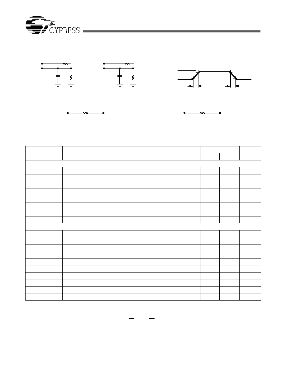
AC Test Loads and Waveforms
(R1 255
MIL)
(R1 255
MIL)
(480
MIL)
(480
MIL)
3.0V
5V
OUTPUT
R1 329
R2 202
30 pF
GND
90%
90%
10%
5 ns
5 ns
5V
OUTPUT
C187≠4
R2 202
5 pF
C187≠5
(a)
(b)
OUTPUT
1.73V
INCLUDING
JIG AND
SCOPE
INCLUDING
JIG AND
SCOPE
R1 329
Equivalent to:
TH… VENIN EQUIVALENT
10%
OUTPUT
1.90V
Military
Commercial
ALL INPUT PULSES
167
125
Switching Characteristics
Over the Operating Range
[6]
7C187-15
7C187-20
Parameter
Description
Min.
Max.
Min.
Max.
Unit
READ CYCLE
t
RC
Read Cycle Time
15
20
ns
t
AA
Address to Data Valid
15
20
ns
t
OHA
Output Hold from Address Change
3
5
ns
t
ACE
CE LOW to Data Valid
15
20
ns
t
LZCE
CE LOW to Low Z
[7]
3
5
ns
t
HZCE
CE HIGH to High Z
[7, 8]
8
8
ns
t
PU
CE LOW to Power Up
0
0
ns
t
PD
CE HIGH to Power Down
15
20
ns
WRITE CYCLE
[9]
t
WC
Write Cycle Time
15
20
ns
t
SCE
CE LOW to Write End
12
15
ns
t
AW
Address Set-Up to Write End
12
15
ns
t
HA
Address Hold from Write End
0
0
ns
t
SA
Address Set-Up to Write Start
0
0
ns
t
PWE
WE Pulse Width
12
15
ns
t
SD
Data Set-Up to Write End
10
10
ns
t
HD
Data Hold from Write End
0
0
ns
t
LZWE
WE HIGH to Low Z
5
5
ns
t
HZWE
WE LOW to High Z
[8]
7
7
ns
Notes:
6.
Test conditions assume signal transition time of 5 ns or less, timing reference levels of 1.5V, input pulse levels of 0 to 3.0V, and output loading of the specified
I
OL
/I
OH
and 30-pF load capacitance.
7.
At any given temperature and voltage condition, t
HZCE
is less than t
LZCE
for any given device.
8.
t
HZCE
and t
HZWE
are specified with C
L
= 5 pF as in part (b) of AC Test Loads. Transition is measured
±
500 mV from steady-state voltage.
9.
The internal write time of the memory is defined by the overlap of CE LOW and WE LOW. Both signals must be LOW to initiate a write and either signal can
terminate a write by going HIGH. The data input set-up and hold timing should be referenced to the rising edge of the signal that terminates the write.
CY7C187
Document #: 38-05044 Rev. **
Page 4 of 9
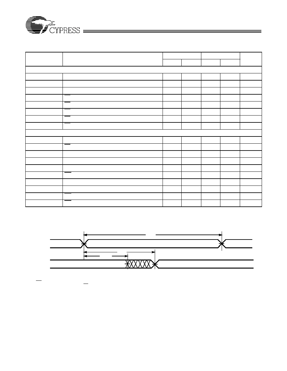
Switching Characteristics
Over the Operating Range
[6]
(continued)
7C187-25
7C187-35
Parameters
Description
Min.
Max.
Min.
Max.
Units
READ CYCLE
t
RC
Read Cycle Time
25
35
ns
t
AA
Address to Data Valid
25
35
ns
t
OHA
Output Hold from Address Change
5
5
ns
t
ACE
CE LOW to Data Valid
25
35
ns
t
LZCE
CE LOW to Low Z
[7]
5
5
ns
t
HZCE
CE HIGH to High Z
[7, 8]
10
15
ns
t
PU
CE LOW to Power Up
0
0
ns
t
PD
CE HIGH to Power Down
20
20
ns
WRITE CYCLE
[9]
t
WC
Write Cycle Time
20
25
ns
t
SCE
CE LOW to Write End
20
25
ns
t
AW
Address Set-Up to Write End
20
25
ns
t
HA
Address Hold from Write End
0
0
ns
t
SA
Address Set-Up to Write Start
0
0
ns
t
PWE
WE Pulse Width
15
20
ns
t
SD
Data Set-Up to Write End
10
15
ns
t
HD
Data Hold from Write End
0
0
ns
t
LZWE
WE HIGH to Low
5
5
ns
t
HZWE
WE LOW to High Z
[8]
7
10
ns
Switching Waveforms
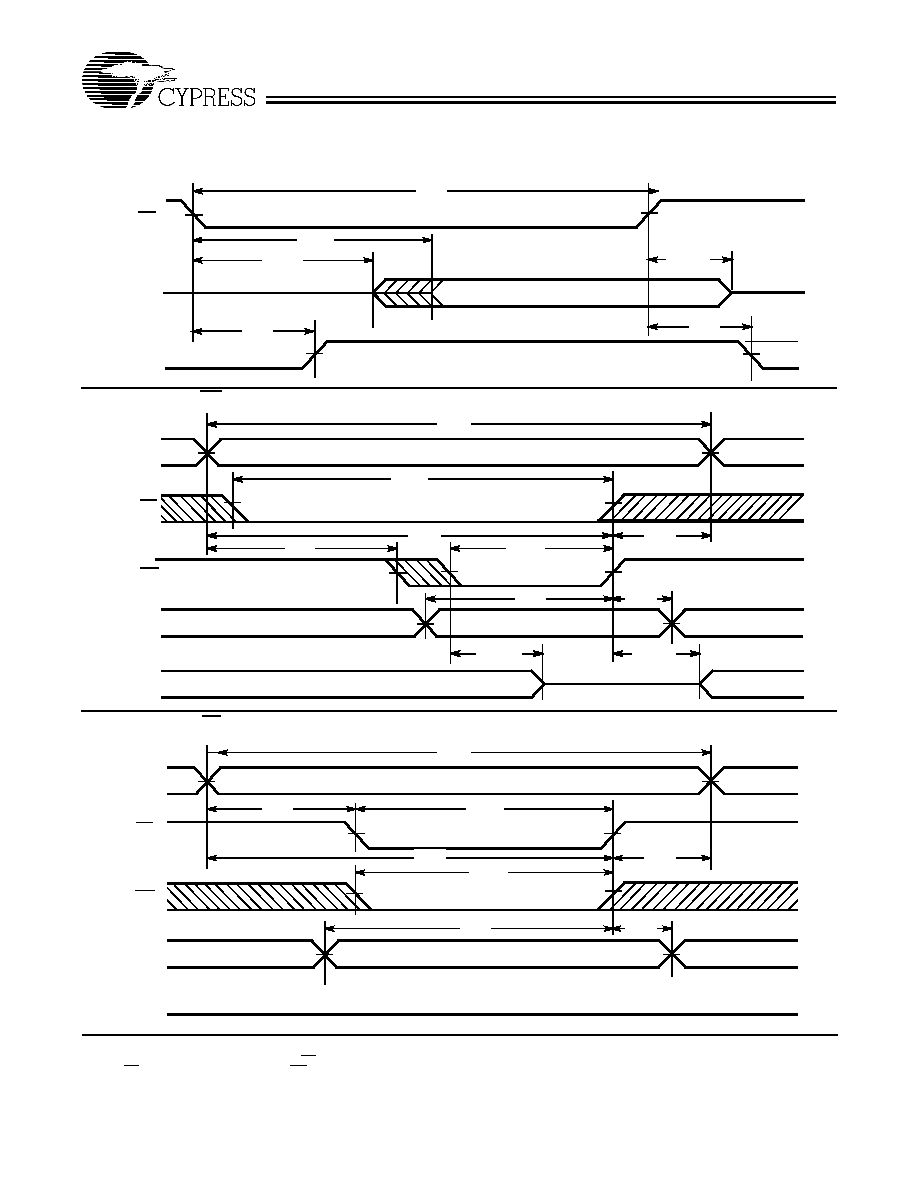
Read Cycle No. 1
[10, 11]
Notes:
10. WE is HIGH for read cycle.
11. Device is continuously selected, CE = V
IL
.
ADDRESS
DATA OUT
PREVIOUS DATA VALID
DATA VALID
t
RC
t
AA
t
OHA
C187≠6
CY7C187
Document #: 38-05044 Rev. **
Page 5 of 9
Read Cycle No. 2
[10, 12]
Notes:
12. Address valid prior to or coincident with CE
transition LOW.
13. If CE goes HIGH simultaneously with WE HIGH, the output remains in a high-impedance state.
Switching Waveforms
50%
50%
DATA VALID
t
RC
t
ACE
t
LZCE
t
PU
DATA OUT
HIGH IMPEDANCE
IMPEDANCE
ICC
ISB
t
HZCE
t
PD
CE
HIGH
t
WC
DATA VALID
DATA UNDEFINED
HIGH IMPEDANCE
t
SCE
t
AW
t
SA
t
PWE
t
HA
t
HD
V
CC
SUPPLY
CURRENT
t
HZWE
t
LZWE
t
SD
CE
WE
DATA IN
DATA OUT
ADDRESS
C187≠7
C187≠8
t
WC
DATA VALID
HIGH IMPEDANCE
t
SCE
t
AW
t
SA
t
PWE
t
HA
t
HD
t
SD
CE
WE
ADDRESS
DATA IN
DATA OUT
C187≠9
Write Cycle No. 1 (WE Controlled)
[11]
Write Cycle No. 2 (CE Controlled)
[11, 13]