Äîêóìåíòàöèÿ è îïèñàíèÿ www.docs.chipfind.ru
256Kx1 Static RAM
CY7C197
Cypress Semiconductor Corporation
·
3901 North First Street
·
San Jose
·
CA 95134
·
408-943-2600
Document #: 38-05049 Rev. **
Revised August 24, 2001
97
Features
· High speed
-- 12 ns
· CMOS for optimum speed/power
· Low active power
-- 880 mW
· Low standby power
-- 220 mW
· TTL-compatible inputs and outputs
· Automatic power-down when deselected
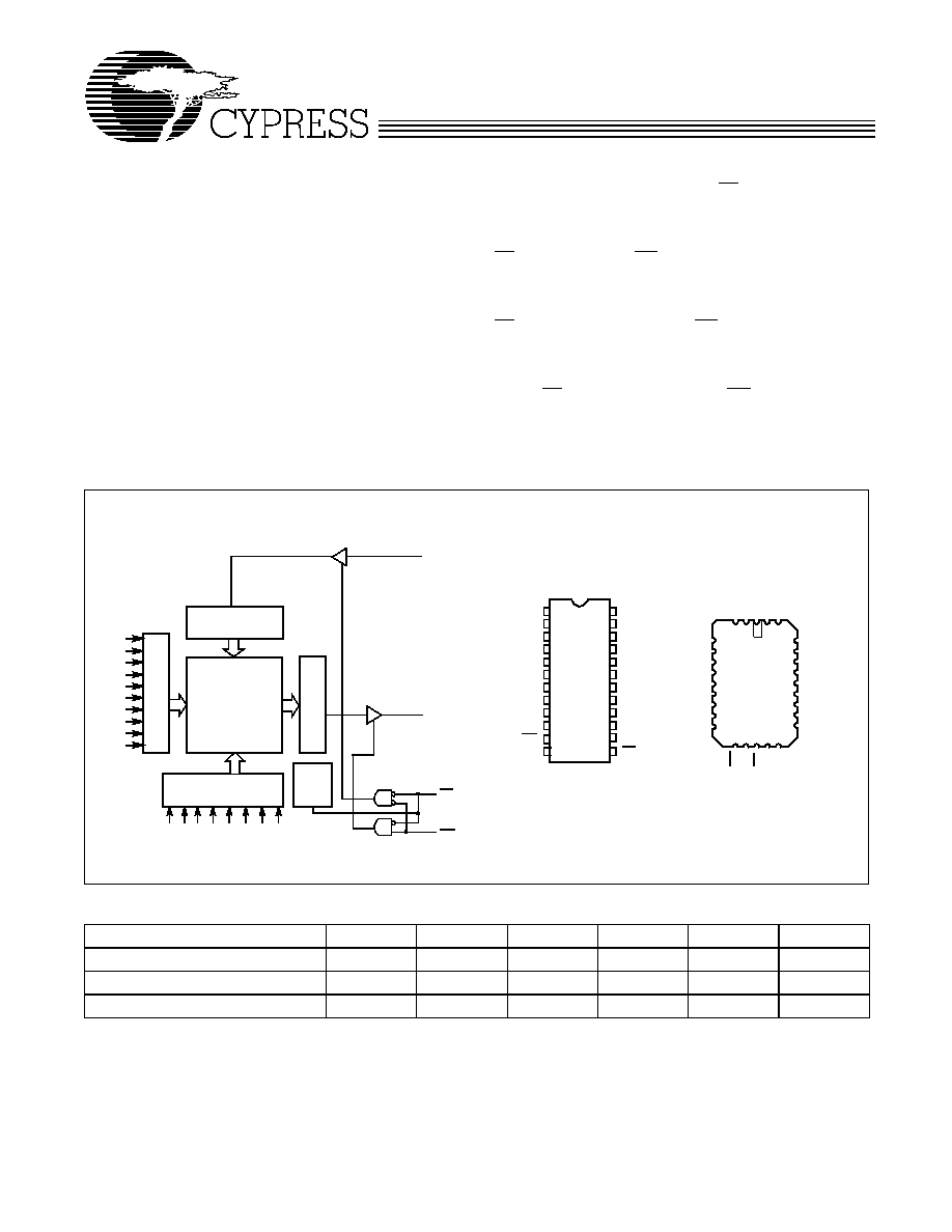
Functional Description
The CY7C197 is a high-performance CMOS static RAM orga-
nized as 256K words by 1 bit. Easy memory expansion is pro-
vided by an active LOW Chip Enable (CE) and three-state driv-
ers. The CY7C197 has an automatic power-down feature,
reducing the power consumption by 75% when deselected.
Writing to the device is accomplished when the Chip Enable
(CE) and Write Enable (WE) inputs are both LOW. Data on the
input pin (D
IN
) is written into the memory location specified on
the address pins (A
0
through A
17
).
Reading the device is accomplished by taking chip enable
(CE) LOW while Write Enable (WE) remains HIGH. Under
these conditions the contents of the memory location specified
on the address pins will appear on the data output (D
OUT
) pin.
The output pin stays in a high-impedance state when Chip
Enable (CE) is HIGH or Write Enable (WE) is LOW.
The CY7C197 utilizes a die coat to insure alpha immunity.
WE
GND
28
Logic Block Diagram
Pin Configurations
1024 x 256
ARRAY
A
1
A
2
A
3
A
4
A
5
A
6
A
7
A
8
COLUMN
DECODER
ROW DECODE
R
SENS
E
AM
PS
POWER
DOWN
WE
CE
4
5
6
7
8
9
10
3 2 1
27
1314151617
26
25
24
23
22
21
20
1
2
3
4
5
6
7
8
9
10
11
14
15
16
20
19
18
17
21
24
23
22
Top View
DIP/SOJ
7C197
A
0
A
1
A
2
A
3
A
4
A
5
A
6
A
7
A
8
CE
V
CC
A
17
A
16
A
15
A
14
A
11
A
10
A
9
D
IN
A
13
A
12
D
OUT
11
12
19
18
A
2
V CC
A
3
A
4
A
5
A
6
A
7
A
8
NC
A
9
GND
WE
7C197
Top View
LCC
12
13
INPUT BUFFER
DO
DI
A
0
A
9
A
10
A
11
A
12
A
17
A
16
A
15
A
14
A
13
CE
D
IN
A
1
A
0
A
17
NC
NC
NC
D
OUT
A
16
A
15
A
14
A
11
A
10
A
13
A
12
C197-1
C197-2
C197-3
Selection Guide
7C197-12
7C197-15
7C197-20
7C197-25
7C197-35
7C197-45
Maximum Access Time (ns)
12
15
20
25
35
45
Maximum Operating Current (mA)
150
140
135
95
95
Maximum Standby Current (mA)
30
30
30
30
30
30
CY7C197
Document #: 38-05049 Rev. **
Page 2 of 10
Maximum Ratings
(Above which the useful life may be impaired. For user guide-
lines, not tested.)
Storage Temperature
.....................................-
65
°
C to +150
°
C
Ambient Temperature with
Power Applied
..................................................-
55
°
C to +125
°
C
Supply Voltage to Ground Potential
(Pin 24 to Pin 12)
.................................................-
0.5V to +7.0V
DC Voltage Applied to Outputs
in High Z State
[1]
....................................... -
0.5V to V
CC
+ 0.5V
DC Input Voltage
[1]
.................................... -
0.5V to V
CC
+ 0.5V
Output Current into Outputs (LOW)............................. 20 mA
Static Discharge Voltage .......................................... >2001V
(per MIL-STD-883, Method 3015)
Latch-Up Current .................................................... >200 mA
Operating Range
Range
Ambient
Temperature
V
CC
Commercial
0
°
C to +70
°
C
5V
±
10%
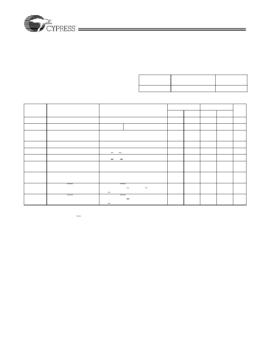
Electrical Characteristics
Over the Operating Range
Parameter
Description
Test Conditions
7C197-12
7C197-15
Unit
Min.
Max.
Min.
Max.
V
OH
Output HIGH Voltage
V
CC
= Min., I
OH
=
-
4.0 mA
2.4
2.4
V
V
OL
Output LOW Voltage
V
CC
= Min.
I
OL
=12.0 mA
0.4
0.4
V
V
IH
Input HIGH Voltage
2.2
V
CC
+ 0.3V
2.2
V
CC
+0.3V
V
V
IL
Input LOW Voltage
[1]
-
0.5
0.8
-
0.5
0.8
V
I
IX
Input Load Current
GND < V
I
< V
CC
-
5
+5
-
5
+5
µ
A
I
OZ
Output Leakage Current
GND < V
O
< V
CC
, Output Disabled
-
5
+5
-
5
+5
µ
A
I
OS
Output Short
Circuit Current
[2]
V
CC
= Max., V
OUT
= GND
-
300
-
300
mA
I
CC
V
CC
Operating
Supply Current
V
CC
= Max., I
OUT
= 0 mA,
f = f
MAX
= 1/t
RC
150
140
mA
I
SB1
Automatic CE Power-Down
Current--TTL Inputs
[3]
Max. V
CC
, CE > V
IH
, V
IN
> V
IH
or
V
IN
< V
IL
, f = f
MAX
30
30
mA
I
SB2
Automatic CE Power-Down
Current--CMOS Inputs
[3]
Max. V
CC
, CE > V
CC
-
0.3V,
V
IN
> V
CC
-
0.3V or V
IN
< 0.3V
10
10
mA
Notes:
1.
V
(min.)
=
-
2.0V for pulse durations of less than 20 ns.
2.
Not more than one output should be shorted at one time. Duration of the short circuit should not exceed 30 seconds.
3.
A pull-up resistor to V
CC
on the CE input is required to keep the device deselected during V
CC
power-up, otherwise I
SB
will exceed values given.
CY7C197
Document #: 38-05049 Rev. **
Page 3 of 10
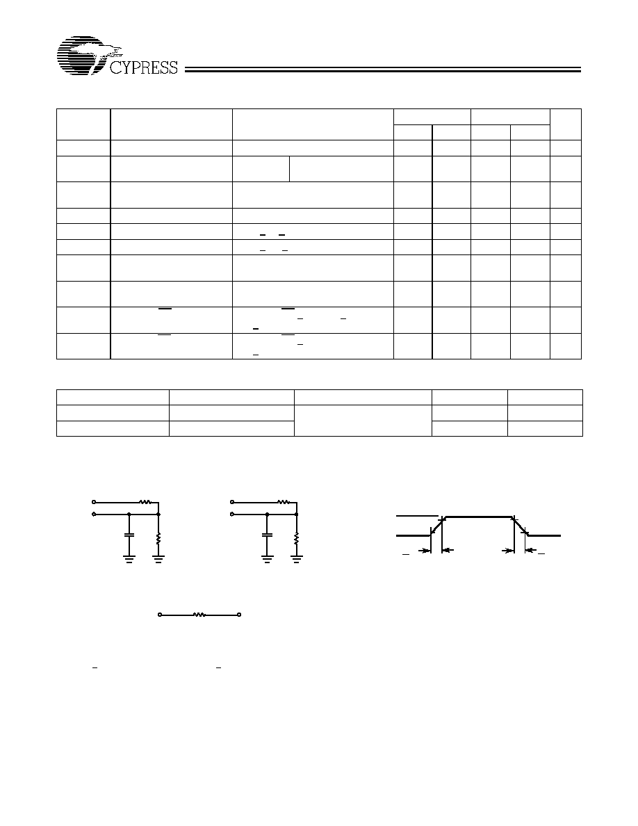
Electrical Characteristics
Over the Operating Range (continued)
Parameter
Description
Test Conditions
7C197-20
7C197-25, 35, 45
Unit
Min.
Max.
Min.
Max.
V
OH
Output HIGH Voltage
V
CC
= Min., I
OH
=
-
4.0 mA
2.4
2.4
V
V
OL
Output LOW Voltage
V
CC
= Min.
I
OL
=12.0mA
0.4
0.4
V
V
IH
Input HIGH Voltage
2.2
V
CC
+ 0.3V
2.2
V
CC
+ 0.3V
V
V
IL
Input LOW Voltage
[1]
-
0.5
0.8
-
0.5
0.8
V
I
IX
Input Load Current
GND < V
I
< V
CC
-
5
+5
-
5
+5
µ
A
I
OZ
Output Leakage Current
GND < V
O
< V
CC
, Output Disabled
-
5
+5
-
5
+5
µ
A
I
OS
Output Short
Circuit Current
[2]
V
CC
= Max., V
OUT
= GND
-
300
-
300
mA
I
CC
V
CC
Operating
Supply Current
V
CC
= Max., I
OUT
= 0 mA,
f = f
MAX
= 1/t
RC
135
95
mA
I
SB1
Automatic CE Power Down
Current--TTL Inputs
[3]
Max. V
CC
, CE > V
IH
, V
IN
> V
IH
or
V
IN
< V
IL
, f = f
MAX
30
30
mA
I
SB2
Automatic CE Power-Down
Current--CMOS Inputs
[3]
Max. V
CC
, CE > V
CC
-
0.3V,
V
IN
> V
CC
-
0.3V or V
IN
< 0.3V
15
15
mA
Capacitance
[4]
Parameter
Description
Test Conditions
Max.
Unit
C
IN
Input Capacitance
T
A
= 25
°
C, f = 1 MHz,
V
CC
= 5.0V
8
pF
C
OUT
Output Capacitance
10
pF
AC Test Loads and Waveforms
[5]
Notes:
4.
Tested initially and after any design or process changes that may affect these parameters.
5.
t
r
= < 3 ns for the -12 and -15 speeds. t
r
= < 5 ns for the -20 and slower speeds.
R2
255
(255
MIL)
R1 329
3.0V
5V
OUTPUT
R1 329
R2
202
(255
MIL)
30 pF
INCLUDING
JIG AND
SCOPE
GND
90%
10%
90%
10%
< t
r
< t
r
5V
OUTPUT
5 pF
INCLUDING
JIG AND
SCOPE
(a)
(b)
OUTPUT
1.90V
Equivalent to:
THÉ VENIN EQUIVALENT
Commercial
ALL INPUT PULSES
C197-4
C197-5
125
CY7C197
Document #: 38-05049 Rev. **
Page 4 of 10
Switching Characteristics
Over the Operating Range
[6]
Parameter
Description
7C197-12
7C197-15
7C197-20
7C197-25
7C197-35
7C197-45
Unit
Min.
Max.
Min.
Max.
Min.
Max.
Min.
Max.
Min.
Max.
Min.
Max.
READ CYCLE
t
RC
Read Cycle Time
12
15
20
25
35
45
ns
t
AA
Address to
Data Valid
12
15
20
25
35
45
ns
t
OHA
Output Hold from
Address Change
3
3
3
3
3
3
ns
t
ACE
CE LOW to
Data Valid
12
15
20
25
35
45
ns
t
LZCE
CE LOW to
Low Z
[7]
3
3
3
3
3
3
ns
t
HZCE
CE HIGH to
High Z
[7, 8]
5
7
0
9
0
11
0
15
0
15
ns
t
PU
CE LOW to
Power-Up
0
0
0
0
0
0
ns
t
PD
CE HIGH to
Power-Down
12
15
20
20
25
30
ns
WRITE CYCLE
[9]
t
WC
Write Cycle Time
12
15
20
25
35
45
ns
t
SCE
CE LOW to
Write End
9
10
15
20
30
40
ns
t
AW
Address Set-Up to
Write End
9
10
15
20
30
40
ns
t
HA
Address Hold from
Write End
0
0
0
0
0
0
ns
t
SA
Address Set-Up to
Write Start
0
0
0
0
0
0
ns
t
PWE
WE Pulse Width
8
9
15
20
25
30
ns
t
SD
Data Set-Up to
Write End
8
9
10
15
17
20
ns
t
HD
Data Hold from
Write End
0
0
0
0
0
0
ns
t
LZWE
WE HIGH to
Low Z
[7]
2
2
3
3
3
3
ns
t
HZWE
WE LOW to
High Z
[7,8]
7
7
0
10
0
11
0
15
0
15
ns
Notes:
6.
Test conditions assume signal transition time of 3 ns or less for -12 and -15 speeds and 5 ns or less for -20 and slower speeds, timing reference levels of
1.5V, input pulse levels of 0 to 3.0V, and output loading of the specified I
OL
/I
OH
and 30-pF load capacitance.
7.
At any given temperature and voltage condition, t
HZCE
is less than t
LZCE
and t
HZWE
is less than t
LZWE
for any given device.
8.
t
HZCE
and t
HZWE
are specified with C
L
= 5 pF as in part (b) in AC Test Loads and Waveforms. Transition is measured
±
500 mV from steady-state voltage.
9.
The internal write time of the memory is defined by the overlap of CE LOW and WE LOW. Both signals must be LOW to initiate a write and either signal can
terminate a write by going HIGH. The data input set-up and hold timing should be referenced to the rising edge of the signal that terminates the write.
CY7C197
Document #: 38-05049 Rev. **
Page 5 of 10
Switching Waveforms
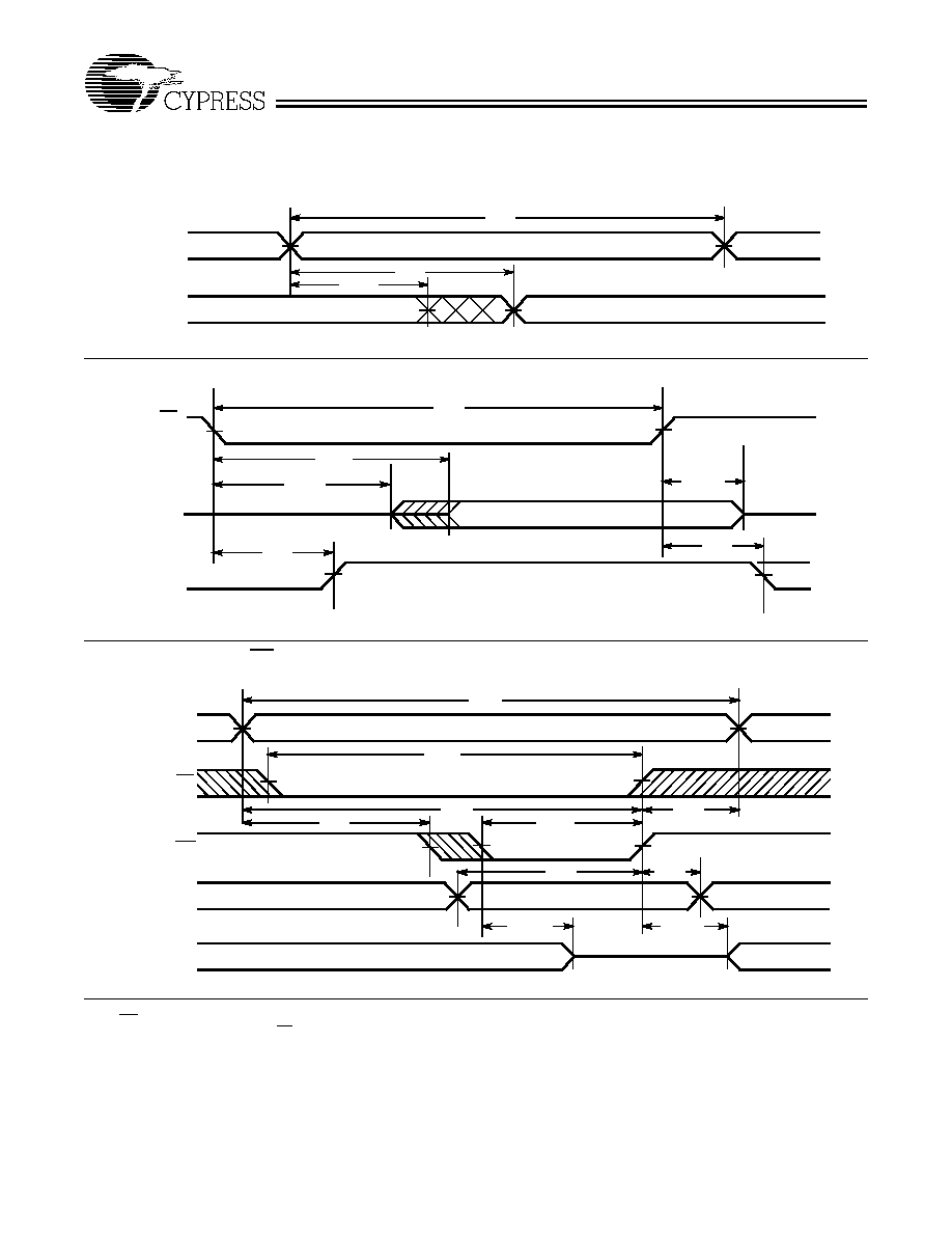
Notes:
10. WE is HIGH for read cycle.
11. Device is continuously selected, CE = V
IL
.
Read Cycle No. 1
ADDRESS
DATA OUT
PREVIOUS DATA VALID
DATA VALID
t
RC
t
AA
t
OHA
C197-6
[10, 11]
Read Cycle No. 2
50%
50%
DATA VALID
t
RC
t
ACE
t
LZCE
t
PU
DATA OUT
HIGH IMPEDANCE
IMPEDANCE
ICC
ISB
t
HZCE
t
PD
CE
HIGH
V
CC
SUPPLY
CURRENT
C197-7
[10]
Write Cycle No. 1 (WE Controlled)
t
WC
DATA VALID
DATA UNDEFINED
HIGH IMPEDANCE
t
SCE
t
AW
t
SA
t
PWE
t
HA
t
HD
t
HZWE
t
LZWE
t
SD
CE
WE
DATA IN
DATA OUT
ADDRESS
C197-8
[9]
CY7C197
Document #: 38-05049 Rev. **
Page 6 of 10
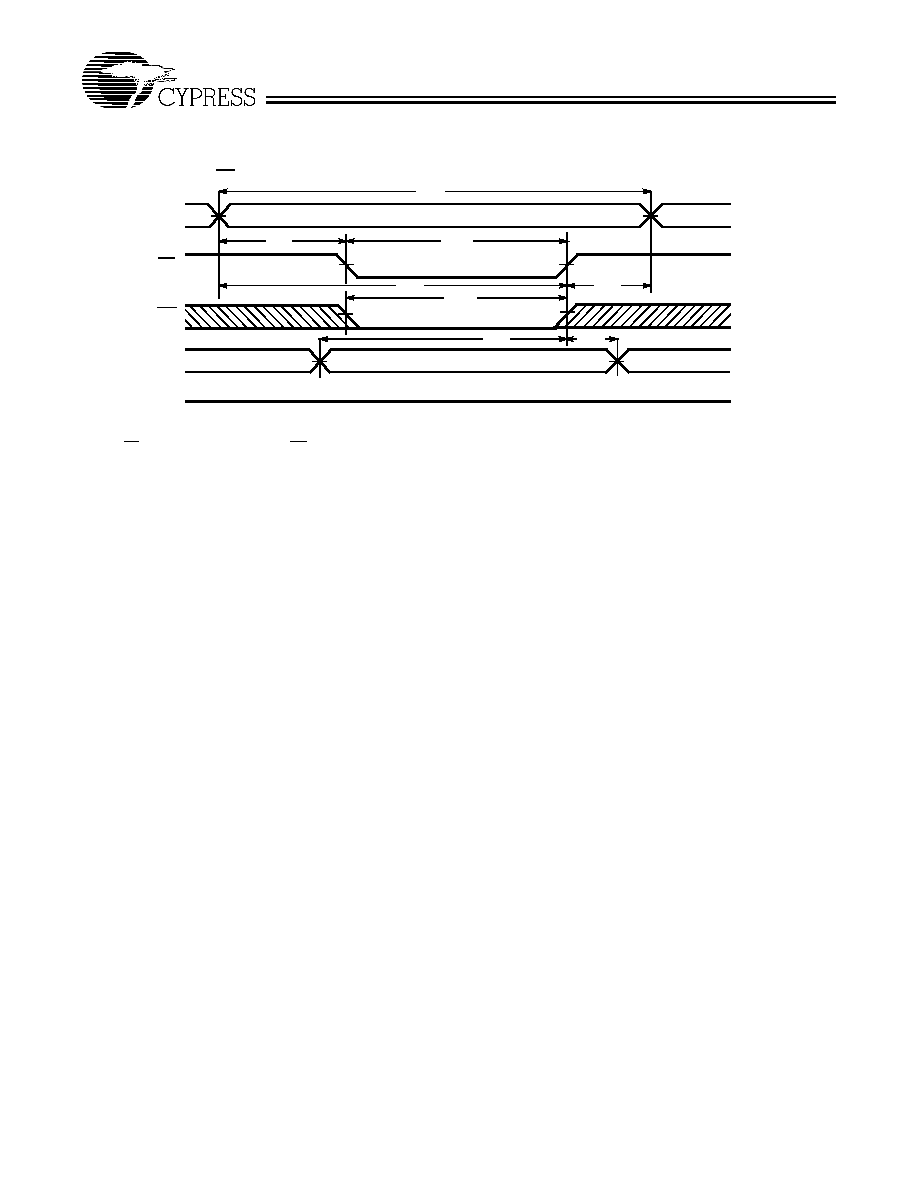
Note:
12. If CE goes HIGH simultaneously with WE HIGH, the output remains in a high-impedance state.
Switching Waveforms (continued)
Write Cycle No. 2 (CE Controlled)
t
WC
DATA VALID
HIGH IMPEDANCE
t
SCE
t
AW
t
SA
t
PWE
t
HA
t
HD
t
SD
ADDRESS
CE
WE
DATA IN
DATA OUT
C197-9
[9, 12]
CY7C197
Document #: 38-05049 Rev. **
Page 7 of 10
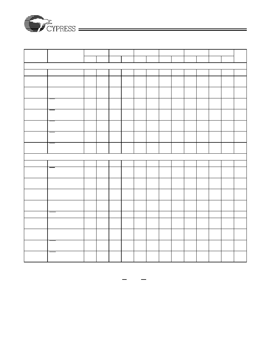
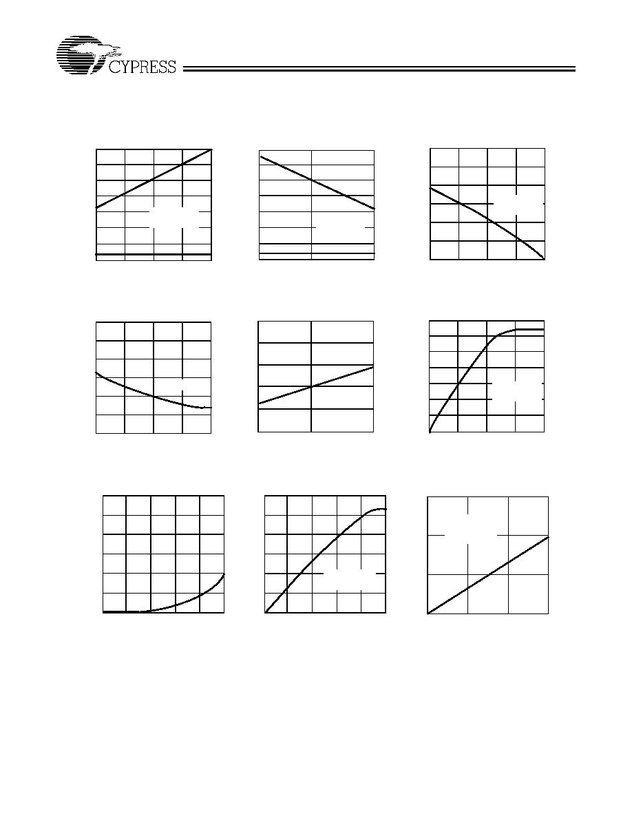
Typical DC and AC Characteristics
1.2
1.4
1.0
0.6
0.4
0.2
4.0
4.5
5.0
5.5
6.0
1.6
1.4
1.2
1.0
0.8
-
55
25
125
-55
25
125
1.2
1.0
0.8
NO
RM
A
L
I
Z
E
D
t
AA
120
100
80
60
40
20
0.0
1.0
2.0
3.0
4.0
OUTP
UT S
O
URCE
CURRE
NT (m
A
)
SUPPLY VOLTAGE(V)
NORMALIZED SUPPLY CURRENT
vs. SUPPLY VOLTAGE
NORMALIZED ACCESS TIME
vs. AMBIENT TEMPERATURE
AMBIENT TEMPERATURE(°C)
NORMALIZED SUPPLY CURRENT
vs. AMBIENT TEMPERATURE
AMBIENT TEMPERATURE(°C)
OUTPUT VOLTAGE(V)
OUTPUT SOURCE CURRENT
vs. OUTPUT VOLTAGE
0.0
0.8
1.4
1.1
1.0
0.9
4.0
4.5
5.0
5.5
6.0
NORM
A
L
IZE
D
t
SUPPLY VOLTAGE(V)
NORMALIZED ACCESS TIME
vs. SUPPLY VOLTAGE
120
140
100
60
40
20
0.0
1.0
2.0
3.0
4.0
OUTP
UT S
I
NK
CURRE
N
T
(m
A
)
0
80
OUTPUT VOLTAGE(V)
OUTPUT SINK CURRENT
vs. OUTPUT VOLTAGE
0.6
0.4
0.2
0.0
NORM
A
L
IZE
D
I
,
I
CC
SB
NORMA
L
I
Z
E
D
I,
I
CC
S
B
I
SB
I
CC
I
CC
V
CC
=5.0V
V
CC
=5.0V
T
A
=25°C
V
CC
=5.0V
T
A
=25°C
I
SB
T
A
=25°C
0.6
0.8
0
AA
1.3
1.2
V
IN
=5.0V
T
A
=25°C
1.4
V
CC
=5.0V
V
IN
=5.0V
3.0
2.5
2.0
1.5
1.0
0.5
0.0
1.0
2.0
3.0
4.0
NORM
A
L
IZ
E
D
I
PO
SUPPLY VOLTAGE (V)
TYPICAL POWER-ON CURRENT
vs. SUPPLY VOLTAGE
30.0
25.0
20.0
15.0
10.0
5.0
0
200
400
600
800
DE
L
T
A t
(
n
s
)
AA
CAPACITANCE (pF)
TYPICAL ACCESS TIME CHANGE
vs. OUTPUT LOADING
1.25
1.00
0.75
10
20
30
40
NORM
A
L
IZ
E
D
I
CC
CYCLE FREQUENCY (MHz)
NORMALIZED I
CC
vs. CYCLE TIME
0.0
5.0
0.0
1000
0.50
V
CC
=4.5V
T
A
=25°C
V
CC
=5.0V
T
A
=25°C
V
IN
=0.5V
CY7C197
Document #: 38-05049 Rev. **
Page 8 of 10
CY7C197 Truth Table
CE
WE
Input/Output
Mode
H
X
High Z
Deselect/Power-Down
L
H
Data Out
Read
L
L
Data In
Write
Ordering Information
Speed
(ns)
Ordering Code
Package
Name
Package Type
Operating
Range
12
CY7C197-12PC
P13
24-Lead (300-Mil) Molded DIP
Commercial
CY7C197-12VC
V13
24-Lead Molded SOJ
15
CY7C197-15PC
P13
24-Lead (300-Mil) Molded DIP
Commercial
CY7C197-15VC
V13
24-Lead Molded SOJ
20
CY7C197-20PC
P13
24-Lead (300-Mil) Molded DIP
Commercial
CY7C197-20VC
V13
24-Lead Molded SOJ
25
CY7C197-25PC
P13
24-Lead (300-Mil) Molded DIP
Commercial
CY7C197-25VC
V13
24-Lead Molded SOJ
35
CY7C197-35PC
P13
24-Lead (300-Mil) Molded DIP
Commercial
CY7C197-35VC
V13
24-Lead Molded SOJ
45
CY7C197-45PC
P13
24-Lead (300-Mil) Molded DIP
Commercial
CY7C197-45VC
V13
24-Lead Molded SOJ
CY7C197
Document #: 38-05049 Rev. **
Page 9 of 10
© Cypress Semiconductor Corporation, 2001. The information contained herein is subject to change without notice. Cypress Semiconductor Corporation assumes no responsibility for the use
of any circuitry other than circuitry embodied in a Cypress Semiconductor product. Nor does it convey or imply any license under patent or other rights. Cypress Semiconductor does not authorize
its products for use as critical components in life-support systems where a malfunction or failure may reasonably be expected to result in significant injury to the user. The inclusion of Cypress
Semiconductor products in life-support systems application implies that the manufacturer assumes all risk of such use and in doing so indemnifies Cypress Semiconductor against all charges.
Package Diagrams
51-85013-A
24-Lead (300-Mil) Molded DIP P13/P13A
24-Lead (300-Mil) Molded SOJ V13
51-85030-A
CY7C197
Document #: 38-05049 Rev. **
Page 10 of 10
Document Title: CY7C197 256K x 1 Static RAM
Document Number: 38-05049
REV.
ECN NO.
Issue
Date
Orig. of
Change
Description of Change
**
107151
09/10/01
SZV
Change from Spec number: 38-00078 to 38-05049