32K x 8 Power Switched and
Reprogrammable PROM
CY7C271A
Cypress Semiconductor Corporation
∑
3901 North First Street
∑
San Jose
∑
CA 95134
∑
408-943-2600
Document #: 38-04013 Rev. *B
Revised December 28, 2002
1CY7C271A
Features
∑ CMOS for optimum speed/power
∑ Windowed for reprogrammability
∑ High speed
-- 25 ns (Commercial)
∑ Low power
-- 275 mW (Commercial)
∑ Super low standby power
-- Less than 85 mW when deselected
∑ EPROM technology 100%programmable
∑ Slim 300-mil package
∑ Direct replacement for bipolar PROMs
∑ Capable of withstanding >4001V static discharge
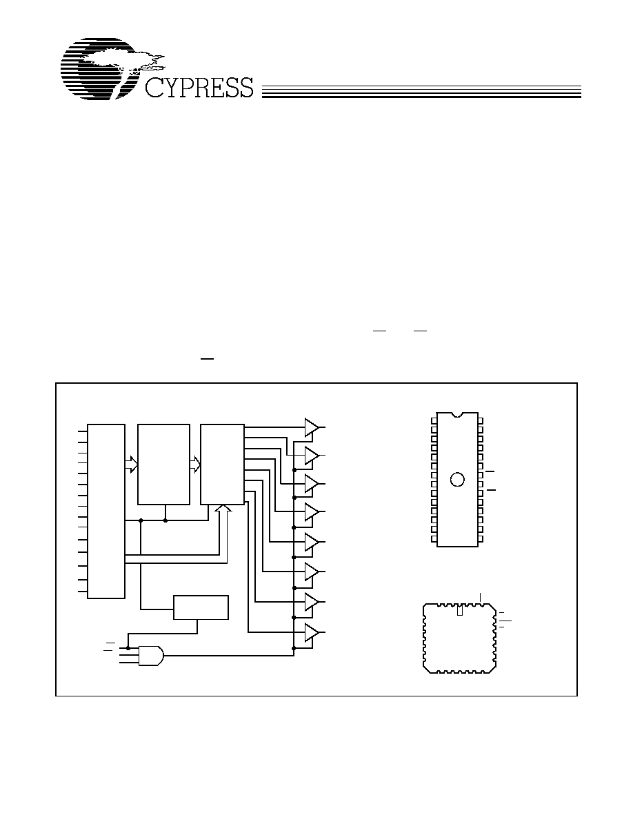
Functional Description
The CY7C271A is a high-performance 32,768-word by 8-bit
CMOS PROM. When disabled (CE HIGH), the 7C271A
automatically powers down into a low-power stand-by mode.
The CY7C271A is packaged in the 300-mil slim package and
is available in a cerDIP package equipped with an erasure
window to provide for reprogrammability. When exposed to UV
light, the PROM is erased and can be reprogrammed. The
memory cells utilize proven EPROM floating gate technology
and byte-wide intelligent programming algorithms.
The CY7C271A offers the advantages of lower power,
superior performance, and programming yield. The EPROM
cell requires only 12.5V for the super voltage, and low current
requirements allow for gang programming. The EPROM cells
allow each memory location to be tested 100% because each
location is written into, erased, and repeatedly exercised prior
to encapsulation. Each PROM is also tested for AC perfor-
mance to guarantee that after customer programming, the
product will meet DC and AC specification limits.
Reading the 7C271A is accomplished by placing active LOW
signals on CS
1
and CE, and an active HIGH on CS
2
. The
contents of the memory location addressed by the address
lines (A
0
≠A
14
) will become available on the output lines
(O
0
≠O
7
).
Logic Block Diagram
Pin Configurations
1
2
3
4
5
6
7
8
9
10
11
12
16
17
18
19
20
24
23
22
21
13
14
25
28
27
26
A
8
A
7
A
6
A
5
A
4
A
3
A
2
A
1
A
0
O
0
O
1
O
2
GND
V
CC
A
11
A
12
A
13
O
7
O
6
O
4
O
5
O
3
A
12
A
11
A
9
A
8
A
7
A
6
A
5
A
4
A
3
A
2
A
1
A
0
POWER-DOWN
O
7
O
6
O
5
O
4
O
3
O
2
O
1
O
0
CE
256 x 1024
PROGRAMABLE
ARRAY
8 x 1 OF 128
MULTIPLEXER
15
A
10
A
13
CS
1
A
9
A
10
A
14
CS
1
CS
2
CE
A
14
CS
2
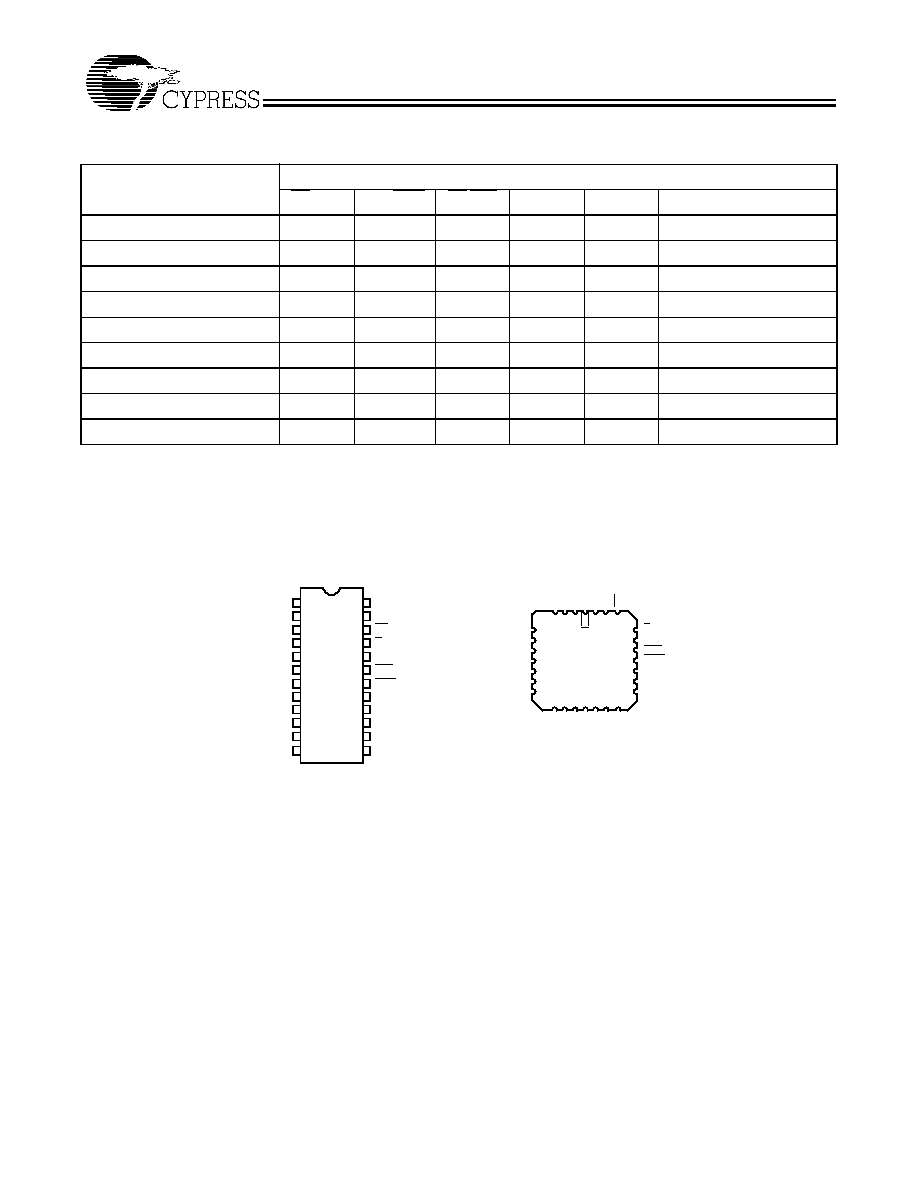
DIP/Flatpack
Y
X
ADDRESS
ADDRESS
28
4
5
6
7
8
9
10
3 2 1
27
13
26
25
24
23
22
21
20
11
12
19
A
5
V
CC
GND
A
6
A
7
O
3
O
1
O
0
18
O
4
O
5
NC
A
0
A
4
A
3
E
NC
NC
NC
CLR
E
S
O
7
O
6
A
2
A
1
CP
O
2
A
8
PS
PLCC
Top View
141516 17
CY7C271A
Document #: 38-04013 Rev. *B
Page 2 of 10
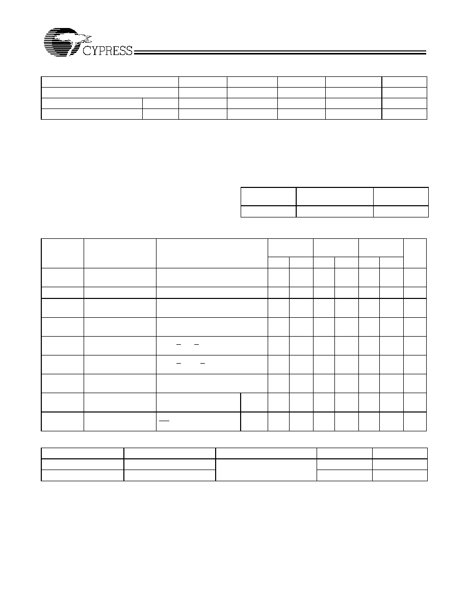
Maximum Ratings
[1]
(Above which the useful life may be impaired. For user guide-
lines, not tested.)
Storage Temperature ................................. ≠65∞C to +150∞C
Ambient Temperature with
Power Applied............................................. ≠55∞C to +125∞C
Supply Voltage to Ground Potential ............... ≠0.5V to +7.0V
DC Voltage Applied to Outputs
in High Z State ............................................... ≠0.5V to +7.0V
DC Input Voltage............................................ ≠3.0V to +7.0V
DC Program Voltage .................................................... 13.0V
Static Discharge Voltage............................................ >4001V
(per MIL-STD-883, Method 3015)
Latch-Up Current..................................................... >200 mA
UV Exposure ................................................ 7258 Wsec/cm
2
Selection Guide
7C271A-25
7C271A-30
7C271A-35
7C271A-45
Unit
Maximum Access Time
25
30
35
45
ns
Maximum Operating Current
Com'l
75
75
50
50
mA
Standby Current
Com'l
15
15
15
15
mA
Operating Range
Range
Ambient
Temperature
V
CC
Commercial
0∞C to +700∞C
5V ±10%
Electrical Characteristics
Over the Operating Range
[2, 3]
Parameter
Description
Test Conditions
7C271A-25
7C271A-30
7C271A-35
7C271A-45
Unit
Min.
Max.
Min.
Max.
Min.
Max.
V
OH
Output HIGH
Voltage
V
CC
= Min., I
OH
= ≠2.0 mA
2.4
2.4
2.4
V
V
OL
Output LOW Voltage
V
CC
= Min., I
OL
= 8.0 mA
0.4
0.4
0.4
V
V
IH
Input HIGH Level
Guaranteed Input Logical HIGH
Voltage for All Inputs
2.0
V
CC
2.0
V
CC
2.0
V
CC
V
V
IL
Input LOW Level
Guaranteed Input Logical LOW
Voltage for All Inputs
0.8
0.8
0.8
V
I
IX
Input Leakage
Current
GND < V
IN
< V
CC
≠10
+10
≠10
+10
≠10
+10
µ
A
I
OZ
Output Leakage
Current
GND < V
OUT
< V
CC
,
Output Disable
≠10
+10
≠10
+10
≠10
+10
µ
A
I
OS
Output Short Circuit
Current
[4]
V
CC
= Max., V
OUT
= GND
≠20
≠90
≠20
≠90
≠20
≠90
mA
I
CC
Power Supply
Current
V
CC
=Max., I
OUT
= 0 mA,
f = 10 MHz
Com'l
75
50
50
mA
I
SB
Stand-By Current
V
CC
=Max.,
CE = V
IH
Com'l
15
15
15
mA
Capacitance
[3]
Parameter
Description
Test Conditions
Max.
Unit
C
IN
Input Capacitance
T
A
= 25
∞
C, f = 1 MHz,
V
CC
= 5.0V
10
pF
C
OUT
Output Capacitance
10
pF
Notes:
1.
The voltage on any input or I/O pin cannot exceed the power pin during power-up.
2.
See the last page of this specification for Group A subgroup testing information.
3.
See Introduction to CMOS PROMs in this Data Book for general information on testing.
4.
For test purposes, not more than one output at a time should be shorted. Short circuit test duration should not exceed 30 seconds.
CY7C271A
Document #: 38-04013 Rev. *B
Page 3 of 10
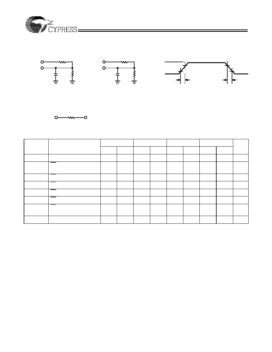
AC Test Loads and Waveforms
90%
10%
3.0V
GND
90%
10%
ALL INPUT PULSES
5V
OUTPUT
30 pF
INCLUDING
JIG AND
SCOPE
5V
OUTPUT
5 pF
INCLUDING
JIG AND
SCOPE
(a) NormalLoad
(b) High-Z Load
5 ns
5 ns
OUTPUT
R1 500
658
MIL
R2 333
403
MIL
200
250
MIL
Equivalent to:
TH… VENIN EQUIVALENT
2.00V Commercial
1.90V MIL
R1 500
658
MIL
R2 333
403
MIL
Switching Characteristics
Over the Operating Range
[2, 3]
7C271A-25
7C271A-30
7C271A-35
7C271A-45
Parameter
Description
Min.
Max.
Min.
Max.
Min.
Max.
Min.
Max.
Unit
t
AA
Address to Output Valid
25
30
35
45
ns
t
ACS
CS
1
/CS
2
Active to
Output Valid
12
18
18
18
ns
t
ACE
CE Active to Output Valid
30
35
35
45
ns
t
HZCS
CS
1
/CS
2
Inactive to High Z
12
18
18
18
ns
t
HZCE
CE Inactive to High Z
12
18
18
18
ns
t
PU
CE Active to Power-Up
0
0
0
0
ns
t
PD
CE Inactive to
Power-Down
30
35
40
40
ns
t
OH
Output Data Hold
0
0
0
0
ns
CY7C271A
Document #: 38-04013 Rev. *B
Page 4 of 10
Erasure Characteristics
Wavelengths of light less than 4000 Angstroms begin to erase
the CY7C271A in the windowed package. For this reason, an
opaque label should be placed over the window if the PROM
is exposed to sunlight or fluorescent lighting for extended
periods of time.
The recommended dose of ultraviolet light for erasure is a
wavelength of 2537 Angstroms for a minimum dose (UV
intensity multiplied by exposure time) of 25 Wsec/cm
2
. For an
ultraviolet lamp with a 12 mW/cm
2
power rating, the exposure
time would be approximately 35 minutes. The CY7C271A
needs to be within 1 inch of the lamp during erasure.
Permanent damage may result if the PROM is exposed to
high-intensity UV light for an extended period of time. 7258
Wsec/cm
2
is the recommended maximum dosage.
Programming Modes
Programming support is available from Cypress as well as
from a number of third-party software vendors. For detailed
programming information, including a listing of software
packages, please see the PROM Programming Information
located at the end of this section. Programming algorithms can
be obtained from any Cypress representative.
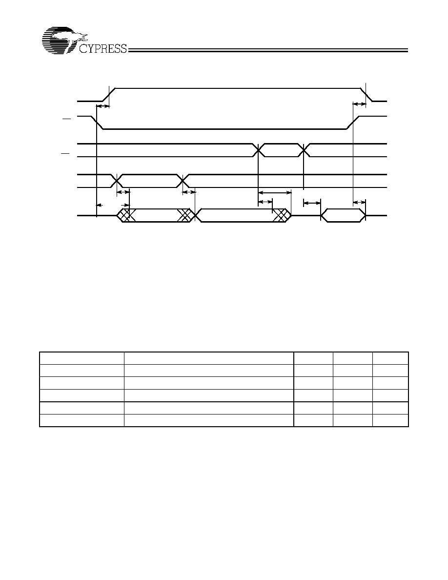
Switching Waveform
t
PU
t
ACE
t
AA
t
PD
CE
O
0
- O
7
A
0
- A
14
CS
1
I
CC
ADDRA
ADDRB
t
AA
DATA A
DATA B
DATA B
t
HZCS
t
ACS
t
HZCE
t
OH
CS
2
ACTIVE
INACTIVE
ACTIVE
Table 1. Programming Electrical Characteristics
Parameter
Description
Min.
Max.
Unit
V
PP
Programming Power Supply
12.5
13
V
I
PP
Programming Supply Current
50
mA
V
IHP
Programming Input Voltage HIGH
3.0
V
CC
V
V
ILP
Programming Input Voltage LOW
≠0.5
0.4
V
V
CCP
Programming V
CC
6.0
6.5
V
CY7C271A
Document #: 38-04013 Rev. *B
Page 5 of 10
Table 2. Mode Selection
Pin Function
[5]
Mode
CS
1
/V
PP
CS
2
/PGM
CE/VFY
A
0
A
9
Data
Read
V
IL
V
IH
V
IL
A
0
A
9
O
7
≠O
0
Output Disable
V
IH
V
IH
V
IL
A
0
A
9
High Z
Output Disable
V
IL
V
IL
V
IL
A
0
A
9
High Z
Stand-by
X
X
V
IH
A
0
A
9
High Z
Program
V
PP
V
ILP
V
IHP
A
0
A
9
D
7
≠D
0
Program Verify
V
PP
V
IHP
V
ILP
A
0
A
9
O
7
≠O
0
Program Inhibit
V
PP
V
IHP
V
IHP
X
X
X
Signature (MFG)
V
ILP
V
ILP
V
ILP
V
ILP
V
HV
[6]
34H
Signature (DEV)
V
ILP
V
ILP
V
ILP
V
IHP
V
HV
[6]
20H
Note:
5.
X can be VIL
or V
IH
.
6.
V
HV
=12
±
0.5V
Programming Pinouts
1
2
3
4
5
6
7
8
9
10
11
12
16
17
18
19
20
24
23
22
21
13
14
A
8
A
7
A
6
A
5
A
4
A
3
A
2
A
1
A
0
D
0
D
1
D
2
GND
V
CC
D
7
D
6
D
4
D
5
D
3
15
PS
E
V
PP
VFY
PGM
28
4
5
6
7
8
9
10
3 2 1
27
1314151617
26
25
24
23
22
21
20
11
12
19
A
5
V CC
GND
A
6
A
7
D
3
D
1
D
0
18
D
4
D
5
NC
A
0
A
4
A
3
A
8
NC
NC
D
7
D
6
A
2
A
1
D
2
E
V
PP
VFY
PGM
NC
PS
DIP
PLCC
Top View
Top View