Äîêóìåíòàöèÿ è îïèñàíèÿ www.docs.chipfind.ru
16K x 16 Reprogrammable PROM
CY7C276
Cypress Semiconductor Corporation
·
3901 North First Street
·
San Jose
·
CA 95134
·
408-943-2600
March 1991 Revised December 1993
1CY 7C27 6
Features
·
0.8-micron CMOS for optimum speed/power
·
High speed (for commercial and military)
-- 25-ns access time
·
16-bit-wide words
·
Three programmable chip selects
·
Programmable output enable
·
44-pin PLCC and 44-pin LCC packages
·
100% reprogrammable in windowed packages
·
TTL-compatible I/O
·
Capable of withstanding greater than 2001V static dis-
charge
Functional Description
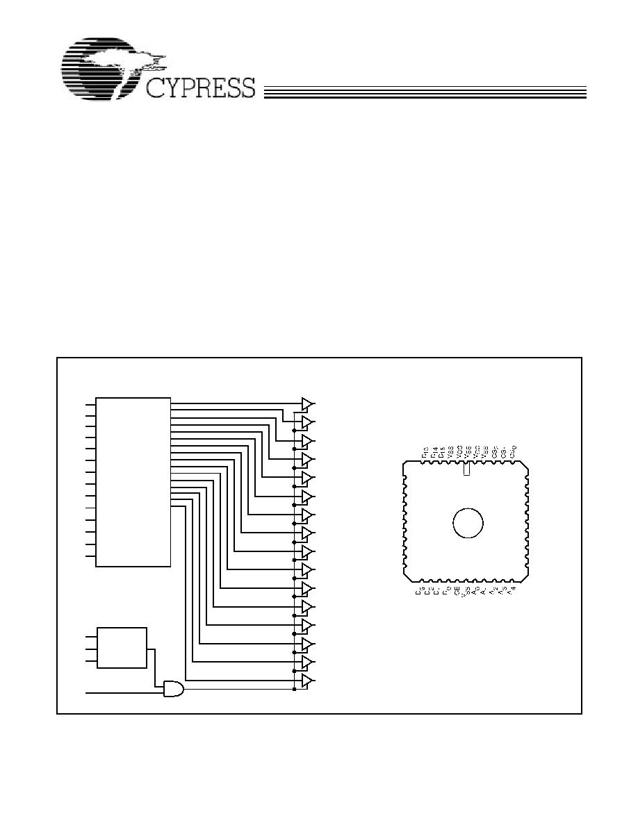
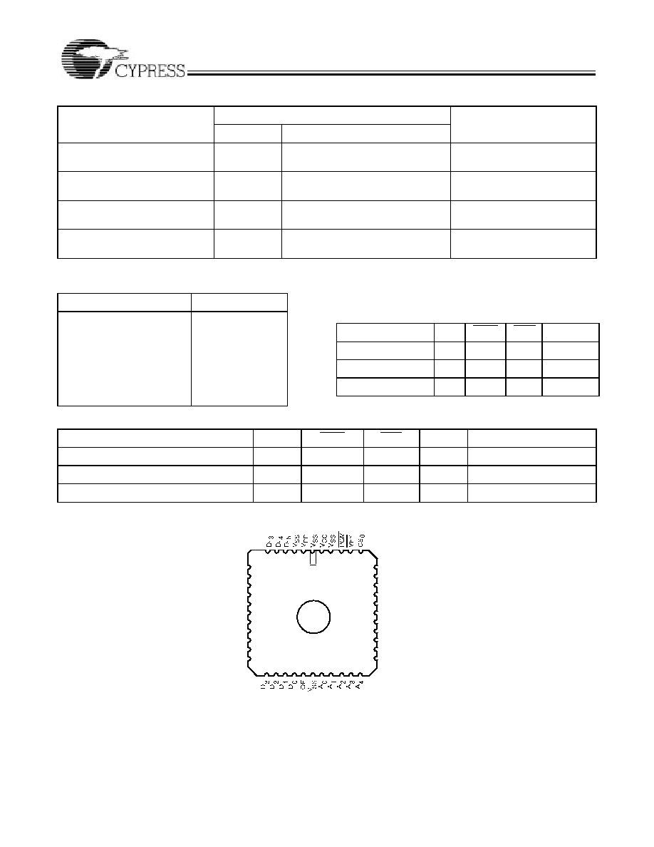
The CY7C276 is a high-performance 16K-word by 16-bit
CMOS PROM. It is available in a 44-pin PLCC/CLCC and a
44-pin LCC packages, and is 100% reprogrammable in win-
dowed packages. The memory cells utilize proven EPROM
floating gate technology and word-wide programming algo-
rithms.
The CY7C276 allows the user to independently program the
polarity of each chip select (CS
2
-
CS
0
). This provides on-chip
decoding of up to eight banks of PROM. The polarity of the
asynchronous output enable pin (OE) is also programmable.
In order to read the CY7C276, all three chip selects must be
active and OE must be asserted. The contents of the memory
location addressed by the address lines (A
13
-
A
0
) will become
available on the output lines (D
15
-
D
0
). The data will remain on
the outputs until the address changes or the outputs are dis-
abled.
C2761
16K x 16
PROGRAMMABLE
ARRAY
CS
DECODE
D
15
D
14
D
13
D
12
D
11
D
10
D
9
D
8
D
7
D
6
D
5
D
4
D
3
D
2
D
1
D
0
LCC/PLCC/CLCC
Top View
C2762
A
13
A
12
A
10
A
9
A
8
A
7
A
6
A
5
A
4
A
3
A
2
A
1
A
0
A
11
CS
0
CS
1
CS
2
OE
1
7
8
9
10
11
12
13
14
15
16
17
39
38
37
36
35
34
33
32
31
30
29
18 19 20 21 22 23 24 25 26 27 28
6 5 4 3 2
44 43 42 41 40
A
13
A
12
A
11
A
10
A
9
V
SS
V
SS
A
8
A
7
A
6
A
5
D
12
D
11
D
10
D
9
D
8
V
SS
V
CC
D
7
D
6
D
5
D
4
Logic Block Diagram
Pin Configuration
CY7C276
2
Maximum Ratings
(Above which the useful life may be impaired. For user guide-
lines, not tested.)
Storage Temperature ................................. 65
°
C to +150
°
C
Ambient Temperature with
Power Applied............................................. 55
°
C to +125
°
C
Supply Voltage to Ground Potential ................ 0.5V to+7.0V
DC Voltage Applied to Outputs
in High Z State ................................................ 0.5V to+7.0V
DC Input Voltage............................................ 3.0V to +7.0V
DC Program Voltage .....................................................13.0V
UV Erasure ...................................................7258 Wsec/cm
2
Static Discharge Voltage ........................................... >2001V
(per MIL-STD-883, Method 3015)
Latch-Up Current ..................................................... >200 mA
Selection Guide
CY7C276-25
CY7C276-30
CY7C276-35
Maximum Access Time (ns)
25
30
35
Maximum Operating
Current (mA)
Commercial
175
175
175
Military
200
200
200
Operating Range
Range
Ambient
Temperature
V
CC
Commercial
0
°
C to +70
°
C
5V
±
10%
Industrial
[1]
40
°
C to +85
°
C
5V
±
10%
Military
[2]
55
°
C to +125
°
C
5V
±
10%
Electrical Characteristics
[3, 4]
Parameter
Description
CY7C276-25
CY7C276-30
CY7C276-35
Unit
Test Conditions
Min.
Max.
V
OH
Output HIGH Voltage
V
CC
= Min., I
OH
= 2.0 mA
2.4
V
V
OL
Output LOW Voltage
V
CC
= Min., I
OL
= 8.0 mA (6.0 mA Mil)
0.4
V
V
IH
Input HIGH Level
Guaranteed Input Logical HIGH Voltage for All Inputs
2.0
V
CC
V
V
IL
Input LOW Level
Guaranteed Input Logical LOW Voltage for All Inputs
3.0
0.8
V
I
IX
Input Leakage Current
GND < V
IN
< V
CC
10
+10
µ
A
V
CD
Input Clamp Diode Voltage
Note 3
µ
A
I
OZ
Output Leakage Current
V
CC
= Max., V
OL
< V
OUT
< V
OH
,
Output Disabled
40
+40
µ
A
I
OS
Output Short Circuit Current
V
CC
= Max., V
OUT
= 0.0V
[5]
20
90
mA
I
CC
Power Supply Current
V
CC
= Max., I
OUT
= 0.0 mA
Com'l
175
mA
Military
200
mA
Capacitance
[3]
Parameter
Description
Test Conditions
Max.
Unit
C
IN
Input Capacitance
T
A
= 25
°
C, f = 1 MHz,
V
CC
= 5.0V
10
pF
C
OUT
Output Capacitance
10
pF
Notes:
1.
Contact a Cypress representative for industrial temperature range specifications.
2.
T
A
is the "instant on" case temperature
3.
See Introduction to CMOS PROMs in this Data Book for general information on testing.
4.
See the last page of this specification for Group A subgroup testing information.
5.
For test purposes, not more than one output at a time should be shorted. Short circuit test duration should not exceed 30 seconds.
CY7C276
3
Erasure Characteristics
The recommended dose of ultraviolet light for erasure is a
wavelength of 2537 Angstroms for a minimum dose (UV inten-
sity multiplied by exposure time) of 25 Wsec/cm2. For an ul-
traviolet lamp with a 12 mW/cm
2
power rating the exposure
time would be approximately 35 minutes. The 7C276 needs to
be within 1 inch of the lamp during erasure. Permanent dam-
age may result if the EPROM is exposed to high-intensity UV
light for an extended period of time. 7258 Wsec/cm
2
is the
recommended maximum dosage.
Wavelengths of light less than 4000 Angstroms begin to erase
the 7C276 in the windowed package. For this reason, an
opaque label should be placed over the window if the EPROM
is exposed to sunlight or fluorescent lighting for extended pe-
riods of time.
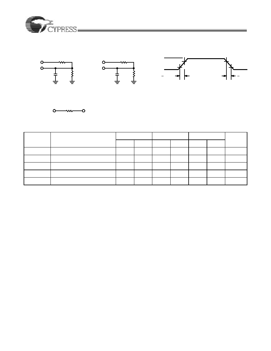
AC Test Loads and Waveforms
C2763
C2764
90%
10%
3.0V
GND
90%
10%
ALL INPUT PULSES
5V
OUTPUT
50 pF
INCLUDING
JIG AND
SCOPE
5V
OUTPUT
5 pF
INCLUDING
JIG AND
SCOPE
(a) Normal Load
(b) High Z Load
< 3 ns
< 3 ns
OUTPUT
2.0V
C2765
(1.9V Mil)
R1 500
(658
MIL)
R1 500
(658
MIL)
R2
333
(403
MIL)
R2
333
(403
MIL)
Equivalent to: THÉ VENIN EQUIVALENT
200
(250
MIL)
Switching Characteristics
Over the Operating Range
[3,4]
CY7C276-25
CY7C276-30
CY7C276-35
Parameter
Description
Min.
Max.
Min.
Max.
Min.
Max.
Unit
t
AA
Address to Output Data Valid
25
30
35
ns
t
CSOV
CS Active to Output Valid
13
15
18
ns
t
CSOZ
CS Inactive to High Z Output
13
15
18
ns
t
OEV
OE Active to Output Valid
11
12
15
ns
t
OEZ
OE Inactive to High Z Output
11
12
15
ns
CY7C276
4
Architecture Configuration Bits
The CY7C276 has four user-programmable options in addition
to the reprogrammable data array. For detailed programming
information contact your local Cypress representative.
The programmable options determine the active polarity for
the three chip selects (CS2 - CS0) and OE. When these con-
trol bits are programmed with a 0 the inputs are active LOW.
When these control bits are programmed with a 1 the inputs
are active HIGH.
Programming Information
Programming support is available from Cypress as well as
from a number of third-party software vendors. For detailed
programming information, including a listing of software pack-
ages, please see the PROM Programming Information located
at the end of this section. Programming algorithms can be ob-
tained from any Cypress representative.
Switching Waveforms
Notes:
6.
CS
2
CS
0
, OE assumed active.
t
OEV
t
CSOV
t
CSOZ
Read Operation Timing Diagram
Chip Select and Output Enable Timing Diagrams
ADDR A
C2766
C2767
ADDR B
DATA A
DATA B
t
AA
t
AA
INACTIVE
ACTIVE
t
OEZ
INACTIVE
A
13
-
A
0
CS
2
-
CS
0
OE
ACTIVE HIGH
D
15
-
D
0
A
13
-
A
0
D
15
-
D
0
VALID
VALID
HIGH Z
[6]
CY7C276
5
Control Word (4000H)
D15
D0
X CS2 CS1 CS0 X X X X X X X X 1 X X OE
Table 1. Control Word for Architecture Configuration
Control Word
Control Option
Bit
Programmed Level
Function
OE
D
0
0=Default
1=Programmed
OE Active LOW
OE Active HIGH
CS
0
D
12
0=Default
1=Programmed
CS
0
Active LOW
CS
0
Active HIGH
CS
1
D
13
0=Default
1=Programmed
CS
1
Active LOW
CS
1
Active HIGH
CS
2
D
14
0=Default
1=Programmed
CS
2
Active LOW
CS
2
Active HIGH
Bit Map
Programmer Address (Hex)
RAM Data
0000
Data
.
.
.
.
.
.
3FFF
Data
4000
Control Word
Table 2. Program Mode Table
Mode
V
PP
PGM
VFY
D
0
-
D
15
Program Inhibit
V
PP
V
IHP
V
IHP
High Z
Program Enable
V
PP
V
ILP
V
IHP
Data
Program Verify
V
PP
V
IHP
V
ILP
Data
Table 3. Configuration Mode Table
Mode
V
PP
PGM
VFY
A
2
D
0
-
D
15
Program Inhibit
V
PP
V
IHP
V
IHP
V
PP
High Z
Program Control Word
V
PP
V
ILP
V
IHP
V
PP
Control Word
Verify Control Word
V
PP
V
IHP
V
ILP
V
PP
Control Word
Figure 1. Programming Pinout
C2768
CY7C276
1
7
8
9
10
11
12
13
14
15
16
17
39
38
37
36
35
34
33
32
31
30
29
18 19 20 21 22 23 24 25 26 27 28
6 5 4 3 2
44 43 42 41 40
A
13
A
12
A
11
A
10
A
9
V
SS
V
SS
A
8
A
7
A
6
A
5
D
12
D
11
D
10
D
9
D
8
V
SS
V
CC
D
7
D
6
D
5
D
4
CY7C276
6
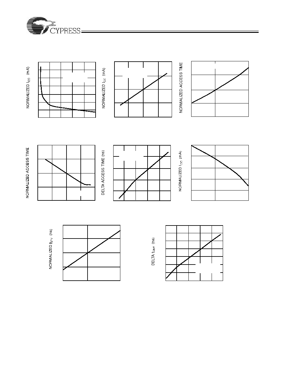
Typical DC and AC Characteristics
1.1
1.2
0.9
0.8
0
100
200
300
400
6
1.4
1.2
1.2
1.1
1.0
0.9
4.0
4.5
5.0
5.5
6.0
ACCESS TIME (ns)
NORMALIZED I
CC
vs.
t
CKA
CYCLE
NORMALIZED I
CC
vs. OUTPUT
VOLTAGE
OUTPUT VOLTAGE (V)
SUPPLYVOLTAGE(V)
NORMALIZED t
CKA
vs. SUPPLY VOLTAGE
0.7
1.0
1.4
1.2
1.0
0.8
-
55
125
AMBIENT TEMPERATURE (
°
C)
NORMALIZED t
CKA
vs. TEMPERATURE
30
35
25
15
10
5
0
200
400
600
0
20
OUTPUT LOAD (pF)
t
OEV
CHANGE vs. OUTPUT
LOADING
1.0
0.8
0.6
T
A
=90
°
C
0.6
25
20
15
10
5
0
200
OUTPUT LOAD (pF)
25
0
800
C2769
0.6
0.5
T
A
=25
°
C
V
CC
=5.5V
500
5.5
5
4.5
4
T
A
=25
°
C
f=f
MAX
V
CC
=4.5V
0.9
400
600
800 1000
T
A
=25
°
C
V
CC
=4.5V
t
CKA
CHANGE
vs. OUTPUT LOADING
0.95
0.90
0.85
-
55
125
AMBIENT TEMPERATURE (
°
C)
NORMALIZED I
CC
vs.
AMBIENT TEMPERATURE
25
V
CC
=5.6V
1.0
1.1
1.1
1.2
1.0
0
0.9
TEMPERATURE(
°
C)
NORMALIZED t
OEV
vs.
TEMPERATURE
V
CC
=4.5V
-
55
125
25
V
CC
=4.5V
T
A
=25
°
C
1000
1.05
CY7C276
7
MILITARY SPECIFICATIONS
Group A Subgroup Testing
Document #: 38-00183-D
Ordering Information
[7]
Speed
(ns)
Ordering Code
Pack-
age
Name
Package Type
Operating
Range
25
CY7C276-25HC
H67
44-Pin Windowed Leaded Chip Carrier
Commercial
CY7C276-25JC
J67
44-Lead Plastic Leaded Chip Carrier
CY7C276-25HMB
H67
44-Pin Windowed Leaded Chip Carrier
Military
CY7C276-25QMB
Q67
44-Pin Windowed Leadless Chip Carrier
30
CY7C276-30HC
H67
44-Pin Windowed Leaded Chip Carrier
Commercial
CY7C276-30JC
J67
44-Lead Plastic Leaded Chip Carrier
CY7C276-30HMB
H67
44-Pin Windowed Leaded Chip Carrier
Military
CY7C276-30QMB
Q67
44-Pin Windowed Leadless Chip Carrier
35
CY7C276-35HC
H67
44-Pin Windowed Leaded Chip Carrier
Commercial
CY7C276-35JC
J67
44-Lead Plastic Leaded Chip Carrier
CY7C276-35HMB
H67
44-Pin Windowed Leaded Chip Carrier
Military
CY7C276-35QMB
Q67
44-Pin Windowed Leadless Chip Carrier
Notes:
7.
Most of the above products are available in industrial temperature range. Contact a Cypress representative for specifications and
product availability.
DC Characteristics
Parameter
Subgroups
V
OH
1, 2, 3
V
OL
1, 2, 3
V
IH
1, 2, 3
V
IL
1, 2, 3
I
IX
1, 2, 3
I
OZ
1, 2, 3
I
CC
1, 2, 3
Switching Characteristics
Parameter
Subgroups
t
AA
7, 8, 9, 10, 11
t
CSOV
7, 8, 9, 10, 11
t
OEV
7, 8, 9, 10, 11
CY7C276
8
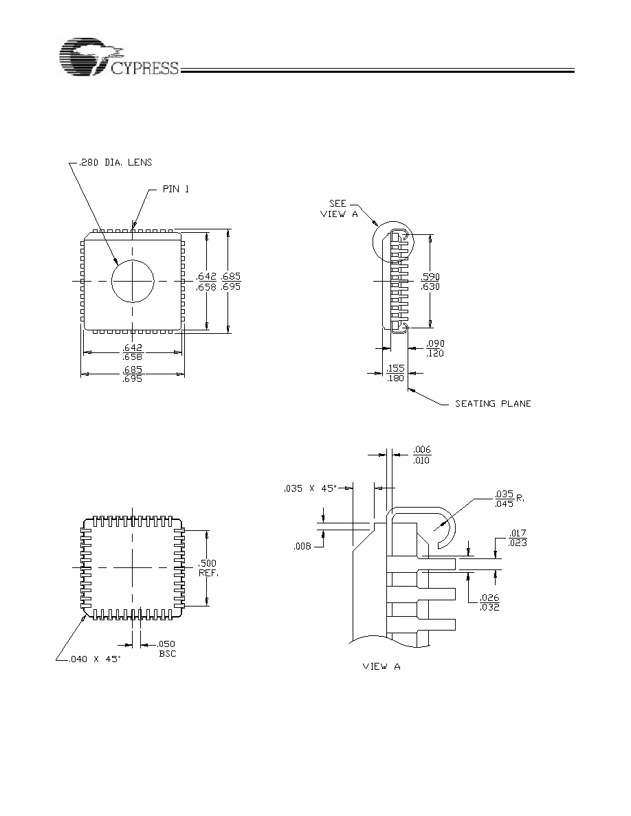
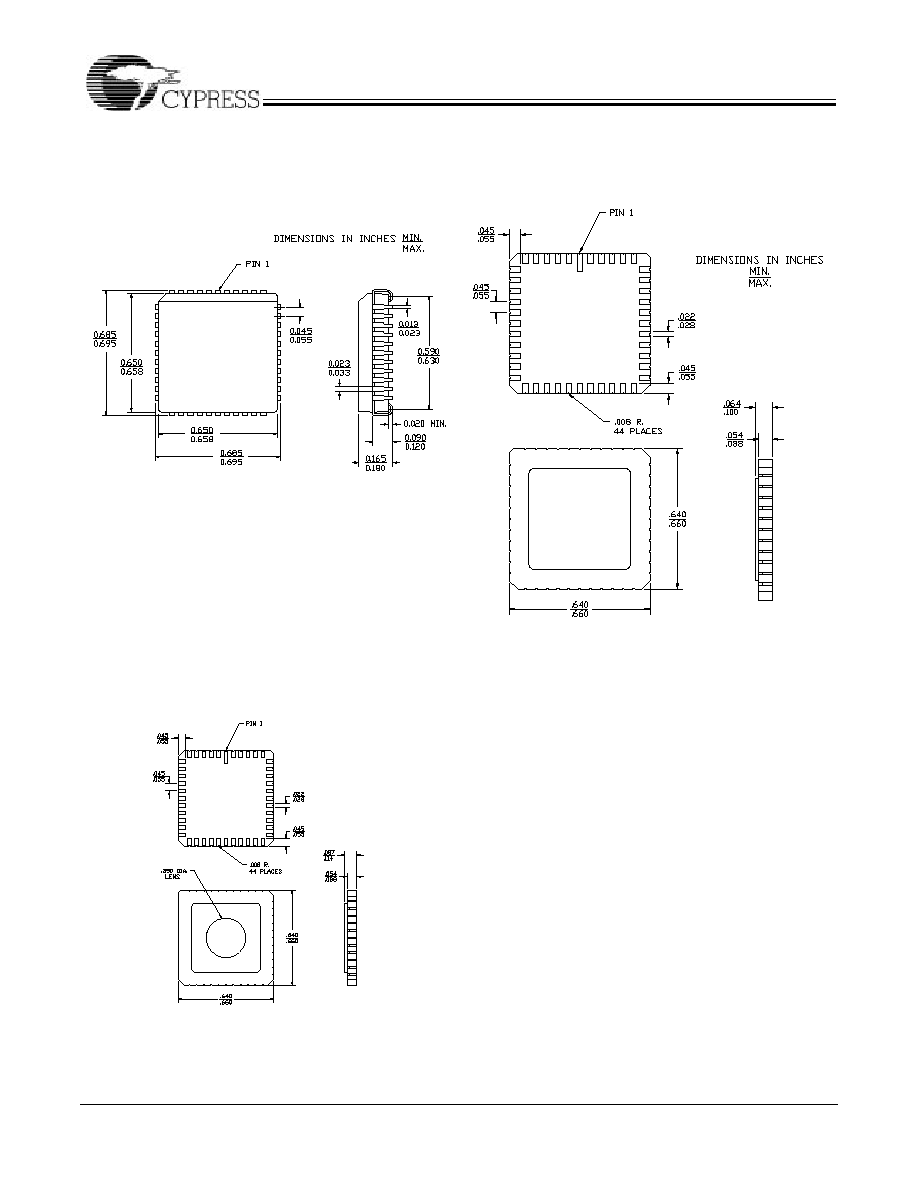
Package Diagrams
44-Pin Windowed Leaded Chip Carrier H67
CY7C276
© Cypress Semiconductor Corporation, 1993. The information contained herein is subject to change without notice. Cypress Semiconductor Corporation assumes no responsibility for the use
of any circuitry other than circuitry embodied in a Cypress Semiconductor product. Nor does it convey or imply any license under patent or other rights. Cypress Semiconductor does not authorize
its products for use as critical components in life-support systems where a malfunction or failure may reasonably be expected to result in significant injury to the user. The inclusion of Cypress
Semiconductor products in life-support systems application implies that the manufacturer assumes all risk of such use and in doing so indemnifies Cypress Semiconductor against all charges.
Package Diagrams (continued)
44-Lead Plastic Leaded Chip Carrier J67
44-Square Leadless Chip Carrier L67
MIL-STD-1835 C-5
44-Pin Windowed Leadless Chip Carrier Q67
MIL-STD-1835 C-5