Untitled Document
1K x 8 PROM
CY7C281A
CY7C282A
Cypress Semiconductor Corporation
·
3901 North First Street
·
San Jose
·
CA 95134
·
408-943-2600
Document #: 38-04003 Rev. **
Revised March 4, 2002
82A
Features
· CMOS for optimum speed/power
· High speed
-- 25 ns (commercial)
-- 30 ns (military)
· Low power
-- 495 mW (commercial)
-- 660 mW (military)
· EPROM technology 100% programmable
· Slim 300-mil or standard 600-mil DIP or 28-pin LCC
· 5V
±
10% V
CC
, commercial and military
· TTL-compatible I/O
· Direct replacement for bipolar PROMs
· Capable of withstanding >2001V static discharge
Functional Description
The CY7C281A and CY7C282A are high-performance
1024-word by 8-bit CMOS PROMs. They are functionally iden-
tical, but are packaged in 300-mil and 600-mil-wide packages
respectively. The CY7C281A is also available in a 28-pin lead-
less chip carrier. The memory cells utilize proven EPROM
floating-gate technology and byte-wide intelligent program-
ming algorithms.
The CY7C281A and CY7C282A are plug-in replacements for
bipolar devices and offer the advantages of lower power, su-
perior performance, and programming yield. The EPROM cell
requires only 12.5V for the super voltage, and low current re-
quirements allow for gang programming. The EPROM cells
allow each memory location to be tested 100% because each
location is written into, erased, and repeatedly exercised prior
to encapsulation. Each PROM is also tested for AC perfor-
mance to guarantee that after customer programming, the
product will meet DC and AC specification limits.
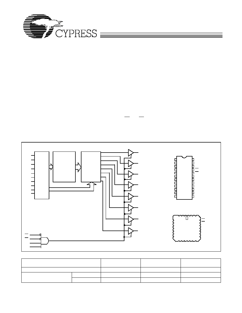
Reading is accomplished by placing an active LOW signal on
CS
1
and CS
2
, and active HIGH signals on CS
3
and CS
4
. The
contents of the memory location addressed by the address
lines (A
0
-
A
9
) will become available on the output lines
(O
0
-
O
7
).
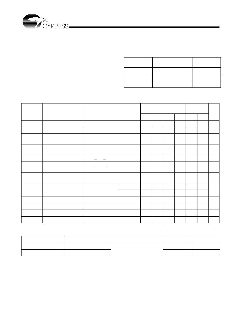
Selection Guide
7C281A-25
7C282A-25
7C281A-30
7C282A-30
7C281A-45
7C282A-45
Maximum Access Time (ns)
25
30
45
Maximum Operating
Current (mA)
Commercial
100
100
90
Military
120
120
LogicBlockDiagram
Pin Configurations
1
2
3
4
5
6
7
8
9
10
11
12
16
17
18
19
20
24
23
22
21
13
14
A8
A7
A6
A5
A4
A3
A2
A1
A0
O0
O1
O2
GND
VCC
O7
O6
O4
O5
O3
A9
A8
A7
A6
A5
A4
A3
A2
A1
A0
O7
O6
O5
O4
O3
O2
O1
O0
CS1
15
COLUMN
DECODER
CS2
CS3
CS4
A9
CS1
CS2
CS3
CS4
28
4
5
6
7
8
9
10
3 2 1
27
1314151617
26
25
24
23
22
21
20
11
12
19
A
5
V CC
GND
A
6
A
7
O
3
O
1
O0
18
O
4
O
5
NC
A0
A4
A3
NC
A
8
A
9
NC
NC
O7
O6
A2
A1
O
2
CS1
CS2
CS3
CS4
DIP
LCC/PLCC
Top View
Top View
7C281A
7C282A
7C281A
ROW
DECODER
PROGRAMMABLE
ARRAY
MULTIPLEXER
CY7C281A
CY7C282A
Document #: 38-04003 Rev. **
Page 2 of 11
Maximum Ratings
(Above which the useful life may be impaired. For user guide-
lines, not tested.)
Storage Temperature
.....................................-
65
°
C to +150
°
C
Ambient Temperature with
Power Applied
..................................................-
55
°
C to +125
°
C
Supply Voltage to Ground Potential
(Pin 24 to Pin 12)
.................................................-
0.5V to +7.0V
DC Voltage Applied to Outputs
in High Z State
.....................................................-
0.5V to +7.0V
DC Input Voltage
.................................................-
3.0V to +7.0V
DC Program Voltage (Pins 18, 20)................................13.0V
Static Discharge Voltage ........................................... >2001V
(per MIL-STD-883, Method 3015)
Latch-Up Current ..................................................... >200 mA
Operating Range
Range
Ambient
Temperature
V
CC
Commercial
0
°
C to +70
°
C
5V
±
10%
Industrial
[1]
-
40
°
C to +85
°
C
5V
±
10%
Military
[2]
-
55
°
C to +125
°
C
5V
±
10%
Electrical Characteristics
Over the Operating Range
[3,4]
7C281A-25
7C282A-25
7C281A-30
7C282A-30
7C281A-45
7C282A-45
Parameter
Description
Test Conditions
Min.
Max.
Min.
Max.
Min.
Max.
Unit
V
OH
Output HIGH Voltage
V
CC
= Min., I
OH
=
-
4.0 mA
2.4
2.4
2.4
V
V
OL
Output LOW Voltage
V
CC
= Min., I
OL
= 16.0 mA
0.4
0.4
0.4
V
V
IH
Input HIGH Level
Guaranteed Input Logical HIGH
Voltage for All Inputs
2.0
2.0
2.0
V
V
IL
Input LOW Level
Guaranteed Input Logical LOW
Voltage for All Inputs
0.8
0.8
0.8
V
I
IX
Input Current
GND < V
IN
< V
CC
-
10
+10
-
10
+10
-
10
+10
µ
A
I
OZ
Output Leakage Current
GND < V
OUT
< V
CC
,
Output Disabled
-
10
+10
-
10
+10
-
10
+10
µ
A
I
OS
Output Short Circuit
Current
[5]
V
CC
= Max., V
OUT
= GND
-
20
-
90
-
20
-
90
-
20
-
90
mA
I
CC
Power Supply Current
V
CC
= Max.,
I
OUT
= 0 mA
Commercial
100
100
90
mA
Military
120
120
V
PP
Program Voltage
12
13
12
13
12
13
V
V
IHP
Program HIGH Voltage
3.0
3.0
3.0
V
V
ILP
Program LOW Voltage
0.4
0.4
0.4
V
I
PP
Program Supply Current
50
50
50
mA
Capacitance
[4]
Parameter
Description
Test Conditions
Max.
Unit
C
IN
Input Capacitance
T
A
= 25
°
C, f = 1 MHz,
V
CC
= 5.0V
10
pF
C
OUT
Output Capacitance
10
pF
Note:
1.
Contact a Cypress representative for industrial temperature range specifications.
2.
T
A
is the "instant on" case temperature.
3.
See the last page of this specification for Group A subgroup testing information.
4.
See "Introduction to CMOS PROMs" in this Data Book for general information on testing.
5.
For test purposes, not more than one output at a time should be shorted. Short circuit test duration should not exceed 30 seconds.
CY7C281A
CY7C282A
Document #: 38-04003 Rev. **
Page 3 of 11
Programming Information
Programming support is available from Cypress as well as
from a number of third party software vendors. For detailed
programming information, including a listing of software pack-
ages, please see the PROM Programming Information located
at the end of this section. Programming algorithms can be ob-
tained from any Cypress representative.
AC Test Loads and Waveforms
[4]
3.0V
5V
OUTPUT
R1 250
R2
167
30pF
INCLUDING
JIG AND
SCOPE
GND
90%
10%
90%
10%
5 ns
5 ns
5V
OUTPUT
5 pF
INCLUDING
JIG AND
SCOPE
(a) Normal Load
(b) High Z Load
OUTPUT
2.0V
Equivalent to:
THÉ VENIN EQUIVALENT
100
R1 250
R2
167
ALL INPUT PULSES
Switching Characteristics
Over the Operating Range
[3,4]
7C281A-25
7C282A-25
7C281A-30
7C282A-30
7C281A-45
7C282A-45
Parameter
Description
Min.
Max.
Min.
Max.
Min.
Max.
Unit
t
AA
Address to Output Valid
25
30
45
ns
t
HZCS
Chip Select Inactive to High Z
15
20
25
ns
t
ACS
Chip Select Active to Output Valid
15
20
25
ns
Switching Waveforms
t
AA
C281A-7
t
HZCS
t
ACS
A
0
-
A
9
ADDRESS
CS
3
, CS
4
CS
1
, CS
2
O
0
-
O
7
DATA
SELECTED
DESELECTED
SELECTED
CY7C281A
CY7C282A
Document #: 38-04003 Rev. **
Page 4 of 11
Table 1. Mode Selection
Pin Function
[6]
Read or Output Disable
A
9
A
0
CS
4
CS
3
CS
2
CS
1
O
7
O
0
Mode
Other
A
9
A
0
PGM
VFY
V
PP
CS
1
D
7
D
0
Read
A
9
A
0
V
IH
V
IH
V
IL
V
IL
O
7
O
0
Output Disable
A
9
A
0
X
X
V
IH
X
High Z
Output Disable
A
9
A
0
X
V
IL
X
X
High Z
Output Disable
A
9
A
0
V
IL
X
X
X
High Z
Output Disable
A
9
A
0
X
X
X
V
IH
High Z
Program
A
9
A
0
V
ILP
V
IHP
V
PP
V
ILP
D
7
D
0
Program Verify
A
9
A
0
V
IHP
V
ILP
V
PP
V
ILP
O
7
O
0
Program Inhibit
A
9
A
0
V
IHP
V
IHP
V
PP
V
ILP
High Z
Intelligent Program
A
9
A
0
V
ILP
V
IHP
V
PP
V
ILP
D
7
D
0
Blank Check
A
9
A
0
V
IHP
V
ILP
V
PP
V
ILP
Zeros
Note:
6.
X = "don't care" but not to exceed V
CC
±
5%.
Figure 1. Programming Pinouts
1
2
3
4
5
6
7
8
9
10
11
12
16
17
18
19
20
24
23
22
21
13
14
A
8
A
7
A
6
A
5
A
4
A
3
A
2
A
1
A
0
D
0
D
1
D
2
GND
V
CC
D
7
D
6
D
4
D
5
D
3
15
A
9
CS
1
V
PP
VFY
PGM
28
4
5
6
7
8
9
10
3 2 1
27
1314151617
26
25
24
23
22
21
20
11
12
19
A
5
V CC
GND
A
6
A
7
D
3
D
1
D
0
18
D
4
D
5
NC
A
0
A
4
A
3
A
8
A
9
NC
NC
D
7
D
6
A
2
A
1
D
2
CS
1
V
PP
VFY
PGM
7C281A
7C282A
NC
DIP
LCC/PLCC
Top View
Top View
7C281A
CY7C281A
CY7C282A
Document #: 38-04003 Rev. **
Page 5 of 11
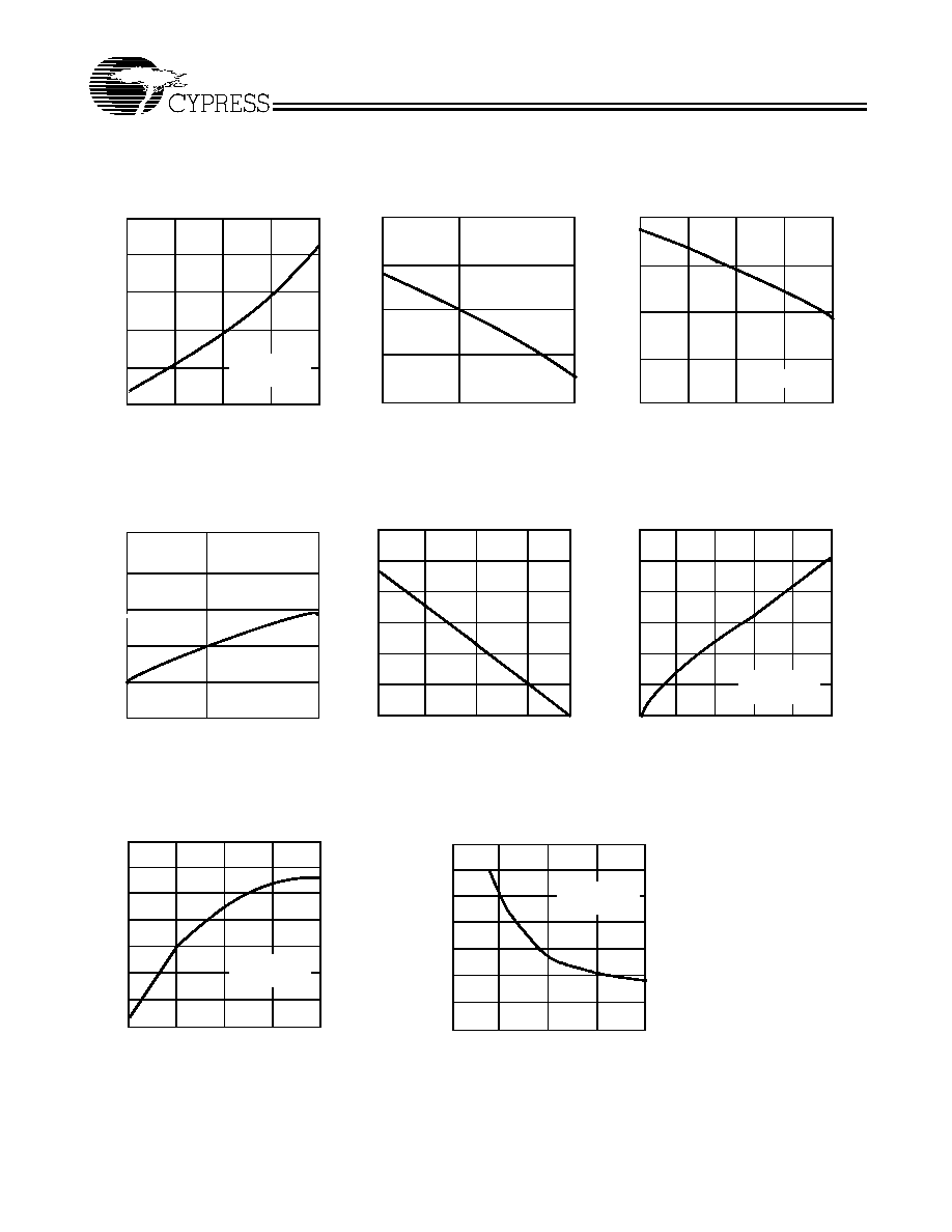
Typical DC and AC Characteristics
1.4
1.6
1.0
0.8
4.0
4.5
5.0
5.5
6.0
-
55
25
125
1.2
1.1
1.2
1.0
0.8
0.6
4.0
4.5
5.0
5.5
6.0
NORM
A
L
IZ
E
D
A
CCE
S
S
TIME
SUPPLYVOLTAGE(V)
NORMALIZED SUPPLY CURRENT
vs. SUPPLY VOLTAGE
NORMALIZED SUPPLY CURRENT
vs. AMBIENT TEMPERATURE
AMBIENT TEMPERATURE(
°
C)
SUPPLYVOLTAGE(V)
NORMALIZED ACCESS TIME
vs. SUPPLY VOLTAGE
0.6
1.2
1.0
0.9
0.8
NORM
A
L
IZ
E
D
I
CC
NORM
A
L
IZ
ED I
CC
T
A
=25
°
C
0.4
T
A
=25
°
C
f = f
MAX
CC
1.6
1.4
1.2
1.0
0.8
-
55
125
NORM
A
L
IZE
D
A
CCE
S
S
T
I
ME
AMBIENT TEMPERATURE (
°
C)
NORMALIZED ACCESSTIME
vs.TEMPERATURE
0.6
60
50
40
30
20
10
0
1.0
2.0
3.0
OUTP
UT S
O
URCE
CU
RRE
NT (mA
)
OUTPUT VOLTAGE (V)
30.0
25.0
20.0
15.0
10.0
5.0
0
200
400
600
800
D
E
L
T
A t
(
n
s
)
AA
CAPACITANCE (pF)
TYPICAL ACCESS TIME CHANGE
vs. OUTPUT LOADING
4.0
0.0
1000
V
CC
=4.5V
T
A
=25
°
C
25
0
OUTPUT SOURCE CURRENT
vs. VOLTAGE
AA
150
175
125
75
50
25
0.0
1.0
2.0
3.0
O
U
T
P
UT S
I
NK
CURR
E
N
T (
m
A
)
0
100
OUTPUT VOLTAGE (V)
OUTPUT SINK CURRENT
vs. OUTPUT VOLTAGE
V
CC
=5.0V
T
A
=25
°
C
4.0
1.00
1.02
0.98
0.94
0.92
0.90
0
25
50
75
100
0.88
0.96
I
CC
vs.CYCLE PERIOD
CYCLE PERIOD (ns)
NORMA
L
I
Z
E
D
I
CC
V
CC
=5.5V
T
A
=25
°
C
CY7C281A
CY7C282A
Document #: 38-04003 Rev. **
Page 6 of 11
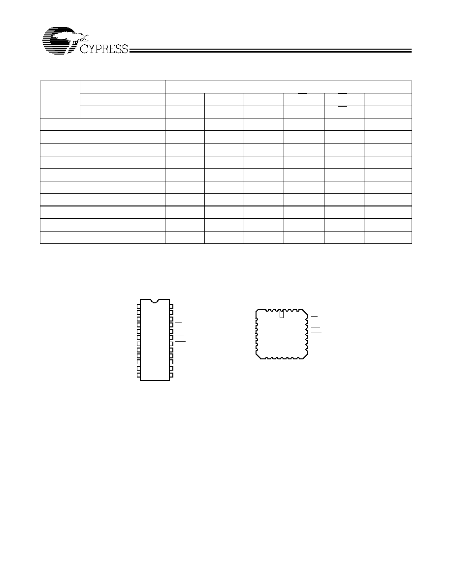
MILITARY SPECIFICATIONS
Group A Subgroup Testing
Ordering Information
Speed
(ns)
Ordering Code
Package
Name
Package Type
Operating
Range
25
CY7C281A-25DC
D14
24-Lead (300-Mil) CerDIP
Commercial
CY7C281A-25JC
J64
28-Lead Plastic Leaded Chip Carrier
CY7C281A-25PC
P13
24-Lead (300-Mil) Molded DIP
30
CY7C281A-30DC
D14
24-Lead (300-Mil) CerDIP
Commercial
CY7C281A-30JC
J64
28-Lead Plastic Leaded Chip Carrier
CY7C281A-30PC
P13
24-Lead (300-Mil) Molded DIP
CY7C281A-30DMB
D14
24-Lead (300-Mil) CerDIP
Military
45
CY7C281A-45DC
D14
24-Lead (300-Mil) CerDIP
Commercial
CY7C281A-45JC
J64
28-Lead Plastic Leaded Chip Carrier
CY7C281A-45PC
P13
24-Lead (300-Mil) Molded DIP
CY7C281A-45DMB
D14
24-Lead (300-Mil) CerDIP
Military
CY7C281A-45KMB
K73
24-Lead Rectangular Cerpack
Speed
(ns)
Ordering Code
Package
Name
Package Type
Operating
Range
25
CY7C282A-25PC
P11
24-Lead (600-Mil) Molded DIP
Commercial
30
CY7C282A-30PC
P11
24-Lead (600-Mil) Molded DIP
Commercial
CY7C282A-30DMB
D12
24-Lead (600-Mil) CerDIP
Military
45
CY7C282A-45PC
P11
24-Lead (600-Mil) Molded DIP
Commercial
CY7C282A-45DMB
D12
24-Lead (600-Mil) CerDIP
Military
DC Characteristics
Parameter
Subgroups
V
OH
1, 2, 3
V
OL
1, 2, 3
V
IH
1, 2, 3
V
IL
1, 2, 3
I
IX
1, 2, 3
I
OZ
1, 2, 3
I
CC
1, 2, 3
Switching Characteristics
Parameter
Subgroups
t
AA
7, 8, 9, 10, 11
t
ACS
7, 8, 9, 10, 11
CY7C281A
CY7C282A
Document #: 38-04003 Rev. **
Page 7 of 11
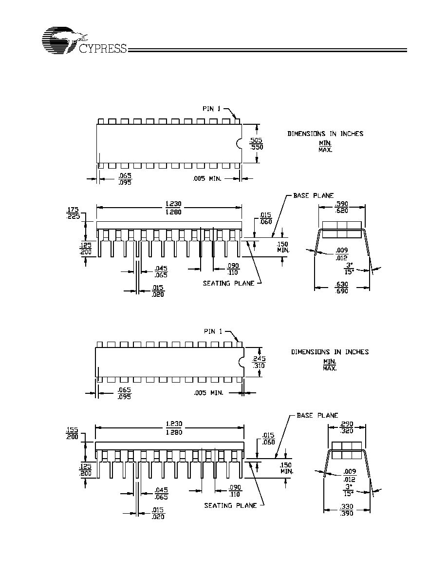
Package Diagrams
24-Lead (600-Mil) CerDIP D12
MIL-STD-1835 D-3 Config. A
51-80038
24-Lead (300-Mil) CerDIP D14
MIL-STD-1835 D- 9 Config.A
51-80031
CY7C281A
CY7C282A
Document #: 38-04003 Rev. **
Page 8 of 11
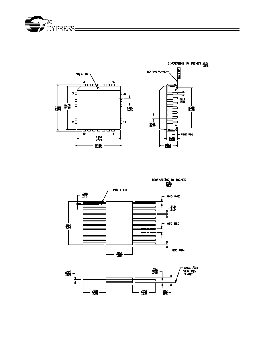
Package Diagrams
(continued)
28-Lead Plastic Leaded Chip Carrier J64
51-85001-A
24-Lead Rectangular Cerpack K73
MIL-STD-1835 F-6 Config. A
51-80060
CY7C281A
CY7C282A
Document #: 38-04003 Rev. **
Page 9 of 11
Package Diagrams
(continued)
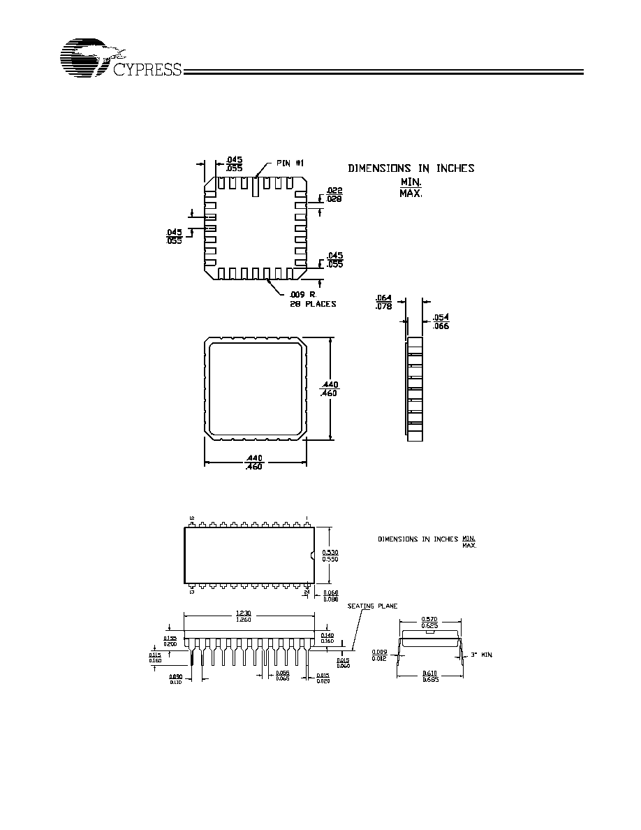
28-Square Leadless Chip Carrier L64
MIL-STD-1835 C-4
51-80051
51-85016-A
24-Lead (600-Mil) Molded DIP P11
CY7C281A
CY7C282A
Document #: 38-04003 Rev. **
Page 10 of 11
© Cypress Semiconductor Corporation, 2002. The information contained herein is subject to change without notice. Cypress Semiconductor Corporation assumes no responsibility for the use
of any circuitry other than circuitry embodied in a Cypress Semiconductor product. Nor does it convey or imply any license under patent or other rights. Cypress Semiconductor does not authorize
its products for use as critical components in life-support systems where a malfunction or failure may reasonably be expected to result in significant injury to the user. The inclusion of Cypress
Semiconductor products in life-support systems application implies that the manufacturer assumes all risk of such use and in doing so indemnifies Cypress Semiconductor against all charges.
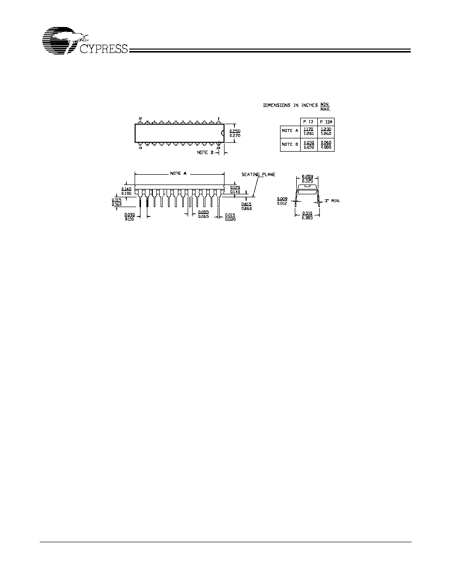
Package Diagrams
(continued)
51-85013-A
24-Lead (300-Mil) Molded DIP P13/P13A

CY7C281A
CY7C282A
Document #: 38-04003 Rev. **
Page 11 of 11
Document Title: CY7C281A, CY7C282A 1K x 8 PROM
Document Number: 38-04003
REV.
ECN NO.
Issue
Date
Orig. of
Change
Description of Change
**
113859
03/06/02
DSG
Change from Spec number: 38-00227 to 38-04003
Document Outline