/home/web/doc/html/cypress/169573
192-Macrocell MAX
®
EPLD
CY7C341B
Cypress Semiconductor Corporation
·
3901 North First Street
·
San Jose
·
CA 95134
·
408-943-2600
Document #: 38-03016 Rev. *B
Revised December 28, 2002
341B
Features
· 192 macrocells in 12 logic array blocks (LABs)
· Eight dedicated inputs, 64 bidirectional I/O pins
· Advanced 0.65-micron CMOS technology to increase
performance
· Programmable interconnect array
· 384 expander product terms
· Available in 84-pin HLCC, PLCC, and PGA packages
Functional Description
The CY7C341B is an Erasable Programmable Logic Device
(EPLD) in which CMOS EPROM cells are used to configure
logic functions within the device. The MAX
®
architecture is
100% user-configurable, allowing the devices to accom-
modate a variety of independent logic functions.
The 192 macrocells in the CY7C341B are divided into 12 Logic
Array Blocks (LABs), 16 per LAB. There are 384 expander
product terms, 32 per LAB, to be used and shared by the
macrocells within each LAB. Each LAB is interconnected with
a programmable interconnect array, allowing all signals to be
routed throughout the chip.
The speed and density of the CY7C341B allows it to be used in a
wide range of applications, from replacement of large amounts of
7400-series TTL logic, to complex controllers and multifunction
chips. With greater than 37 times the functionality of 20-pin PLDs,
the CY7C341B allows the replacement of over 75 TTL devices. By
replacing large amounts of logic, the CY7C341B reduces board
space, part count, and increases system reliability.
Each LAB contains 16 macrocells. In LABs A, F, G, and L, 8
macrocells are connected to I/O pins and eight are buried,
while for LABs B, C, D, E, H, I, J, and K, four macrocells are
connected to I/O pins and 12 are buried. Moreover, in addition
to the I/O and buried macrocells, there are 32 single product
term logic expanders in each LAB. Their use greatly enhances
the capability of the macrocells without increasing the number
of product terms in each macrocell.
Logic Array Blocks
There are 12 logic array blocks in the CY7C341B. Each LAB consists
of a macrocell array containing 16 macrocells, an expander product
term array containing 32 expanders, and an I/O block. The LAB is
fed by the programmable interconnect array and the dedicated
input bus. All macrocell feedbacks go to the macrocell array, the
expander array, and the programmable interconnect array.
Expanders feed themselves and the macrocell array. All I/O
feedbacks go to the programmable interconnect array so that they
may be accessed by macrocells in other LABs as well as the macro-
cells in the LAB in which they are situated.
Externally, the CY7C341B provides eight dedicated inputs, one of
which may be used as a system clock. There are 64 I/O pins that
may be individually configured for input, output, or bidirectional data
flow.
Programmable Interconnect Array
The Programmable Interconnect Array (PIA) solves inter-
connect limitations by routing only the signals needed by each
logic array block. The inputs to the PIA are the outputs of every
macrocell within the device and the I/O pin feedback of every
pin on the device.
Unlike masked or programmable gate arrays, which induce
variable delay dependent on routing, the PIA has a fixed delay.
This eliminates undesired skews among logic signals, which
may cause glitches in internal or external logic. The fixed
delay, regardless of programmable interconnect array config-
uration, simplifies design by assuring that internal signal
skews or races are avoided. The result is ease of design imple-
mentation, often in a single pass, without the multiple internal
logic placement and routing iterations required for a program-
mable gate array to achieve design timing objectives.
Design Recommendations
For proper operation, input and output pins must be
constrained to the range GND < (V
IN
or V
OUT
) < V
CC
. Unused
inputs must always be tied to an appropriate logic level (either V
CC
or GND). Each set of V
CC
and GND pins must be connected
together directly at the device. Power supply decoupling capacitors
of at least 0.2
µ
F must be connected between V
CC
and GND. For
the most effective decoupling, each V
CC
pin should be separately
decoupled to GND, directly at the device. Decoupling capacitors
should have good frequency response, such as monolithic ceramic
types.
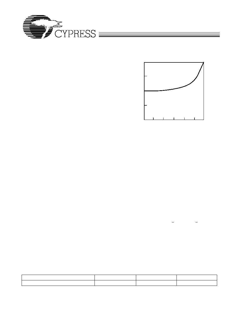
400
300
200
100
1 kHz
10 kHz
100 kHz
1 MHz
I
CC
MAXIMUM FREQUENCY
10 MHz
0
50 MHz
100 Hz
ACT
I
V
E
(mA
) T
y
p.
V
CC
= 5.0V
Room Temp.
Typical I
CC
vs. f
MAX
Selection Guide
7C341B-25
7C341B-35
Unit
Maximum Access Time
25
35
ns
CY7C341B
Document #: 38-03016 Rev. *B
Page 2 of 11
Design Security
The CY7C341B contains a programmable design security
feature that controls the access to the data programmed into
the device. If this programmable feature is used, a proprietary
design implemented in the device cannot be copied or
retrieved. This enables a high level of design control to be
obtained since programmed data within EPROM cells is
invisible. The bit that controls this function, along with all other
program data, may be reset simply by erasing the device.
The CY7C341B is fully functionally tested and guaranteed through
complete testing of each programmable EPROM bit and all internal
logic elements thus ensuring 100% programming yield.
The erasable nature of these devices allows test programs to
be used and erased during early stages of the production flow.
The devices also contain on-board logic test circuitry to allow
verification of function and AC specification once encapsu-
lated in non-windowed packages.
0
1
2
3
4
I
O
U
TP
UT
CURR
E
N
T (
m
A
)
T
Y
P
I
CA
L
V
O
OUTPUT VOLTAGE (V)
250
200
150
100
50
5
O
I
OH
I
OL
V
CC
= 5.0V
Room Temp.
Output Drive Current
P
I
A
MACROCELL 1
MACROCELL 2
MACROCELL 3
MACROCELL 4
MACROCELL 5
MACROCELL 6
MACROCELL 7
MACROCELL 8
MACROCELL97
MACROCELL98
MACROCELL99
MACROCELL 100
MACROCELL 101
MACROCELL 102
MACROCELL 103
MACROCELL 104
MACROCELL 916
MACROCELL 105112
MACROCELL 17
MACROCELL 18
MACROCELL 19
MACROCELL 20
MACROCELL 113
MACROCELL 114
MACROCELL 115
MACROCELL 116
MACROCELL 2132
MACROCELL 117128
MACROCELL 33
MACROCELL 34
MACROCELL 35
MACROCELL 36
MACROCELL 129
MACROCELL 130
MACROCELL 131
MACROCELL 132
MACROCELL 3748
MACROCELL 133144
MACROCELL 49
MACROCELL 50
MACROCELL 51
MACROCELL 52
MACROCELL 145
MACROCELL 146
MACROCELL 147
MACROCELL 148
MACROCELL 5364
MACROCELL 149160
MACROCELL 65
MACROCELL 66
MACROCELL 67
MACROCELL 68
MACROCELL 161
MACROCELL 162
MACROCELL 163
MACROCELL 164
MACROCELL 6980
MACROCELL 165176
MACROCELL 81
MACROCELL 82
MACROCELL 83
MACROCELL 84
MACROCELL 85
MACROCELL 86
MACROCELL 87
MACROCELL 88
MACROCELL 177
MACROCELL 178
MACROCELL 179
MACROCELL 180
MACROCELL 181
MACROCELL 182
MACROCELL 183
MACROCELL 184
MACROCELL 8996
MACROCELL 185192
INPUT
(C6) 84
INPUT
(C7) 83
INPUT
(L7) 44
INPUT
(J7) 43
1 (A6)
INPUT/CLK
2 (A5)
INPUT
41 (K6)
INPUT
42 (J6)
INPUT
4
(C5)
5
(A4)
6
(B4)
7
(A3)
8
(A2)
9
(B3)
10
(A1)
11
(B2)
12 (C2)
13 (B1)
14 (C1)
15 (D2)
16
(D1)
17
(E3)
20
(F2)
21
(F3)
22
(G3)
23
(G1)
25
(F1)
26
(H1)
27
(H2)
28
(J1)
29
(K1)
30
(J2)
31
(L1)
32
(K2)
33
(K3)
34
(L2)
35
(L3)
36
(K4)
37
(L4)
38
(J5)
46 (L6)
47 (L8)
48 (K8)
49 (L9)
50 (L10)
51 (K9)
52 (L11)
53 (K10)
54 (J10)
55 (K11)
56 (J11)
57 (H10)
58 (H11)
59 (F10)
62 (G9)
63 (F9)
64 (F11)
65 (E11)
67 (E9)
68 (D11)
69 (D10)
70 (C11)
71 (B11)
72 (C10)
73 (A11)
74 (B10)
75 (B9)
76 (A10)
77 (A9)
78 (B8)
79 (A8)
80 (B6)
SYSTEMCLOCK
3, 24, 45, 66 (B5, G2, K7, E10)
18, 19, 39, 40, 60, 61, 81, 82 (E1, E2, K5, L5, G10, G11, A7, B7)
V
CC
GND
() PERTAIN TO 84-PIN PGA PACKAGE
LAB A
LAB B
LAB C
LAB D
LAB E
LAB F
LAB G
LAB H
LAB I
LAB J
LAB K
LAB L
Logic Block Diagram
CY7C341B
Document #: 38-03016 Rev. *B
Page 3 of 11
Pin Configurations
I/O
Top View
PLCC/HLCC
9 8
6
7
5
13
14
12
11 10
49
48
58
59
60
23
24
26
25
27
15
16
47
46
4 3
28
33
20
21
19
18
17
22
34 35
37
36
38 39
42
41
43 44 45
40
66
65
63
64
62
61
V
CC
7C341B
67
68
69
74
72
73
71
70
84 83
81
82
80
2 1
79
I/O
INP
U
T
I/O
INP
U
T
/
CLK
INP
U
T
INP
U
T
GND
GND
I/O
I/O
I/O
I/O
I/O
I/O
I/O
I/O
I/O
I/O
I/O
I/O
I/O
I/O
I/O
I/O
GND
I/O
I/O
I/O
I/O
V
CC
V
CC
INP
U
T
GND
GND
INP
U
T
I/O
I/O
I/O
I/O
I/O
I/O
I/O
I/O
I/O
I/O
I/O
I/O
I/O
I/O
I/O
I/O
I/O
I/O
GND
I/O
V
CC
I/O
I/O
I/O
I/O
I/O
I/O
I/O
I/O
I/O
I/O
V
CC
INPUT
INPUT/
CLK
GND
I/O
I/O
I/O
I/O
V
CC
I/O
I/O
I/O
GND
GND
I/O
I/O
I/O
I/O
I/O
I/O
I/O
I/O
I/O
I/O
I/O
V
CC
INPUT
I/O
GND
GND
I/O
I/O
I/O
I/O
I/O
I/O
I/O
I/O
I/O
I/O
V
CC
I/O
I/O
I/O
GND
GND
I/O
I/O
I/O
I/O
I/O
I/O
PGA
Bottom View
7C341B
INPUT
GND
I/O
I/O
I/O
I/O
I/O
I/O
I/O
L
K
J
H
G
F
E
D
C
B
A
1
2
3
4
5
6
7
8
9
10
11
I/O
I/O
I/O
I/O
I/O
INPUT INPUT
INPUT
INPUT
I/O
I/O
I/O
I/O
I/O
I/O
I/O
I/O
53
52
51
50
30
29
31
32
I/O
I/O
I/O
I/O
I/O
I/O
I/O
I/O
54
55
56
57
I/O
I/O
I/O
I/O
77
78
76 75
I/O
I/O
I/O
I/O
I/O
GND
INP
U
T
INP
U
T
GND
I/O
Figure 1. CY7C341B Internal Timing Model
LOGIC ARRAY
CONTROL DELAY
t
LAC
EXPANDER
DELAY
t
EXP
CLOCK
DELAY
t
IC
t
RD
t
COMB
t
LATCH
INPUT
DELAY
t
IN
PIA
DELAY
t
PIA
REGISTER
OUTPUT
DELAY
t
OD
t
XZ
t
ZX
LOGIC ARRAY
DELAY
t
LAD
LOGIC ARRAY
DELAY
t
FD
I/O DELAY
t
IO
INPUT/
OUTPUT
INPUT
SYSTEM CLOCK DELAY t
ICS
t
RH
t
RSU
t
PRE
t
CLR
CY7C341B
Document #: 38-03016 Rev. *B
Page 4 of 11
Maximum Ratings
(Above which the useful life may be impaired. For user guide-
lines, not tested.)
Storage Temperature
.......................................-
65
°
C to +135
°
C
Ambient Temperature with
Power Applied.............................................. 65
°
C to +135
°
C
Maximum Junction Temperature
(Under Bias)................................................................. 150
°
C
Supply Voltage to Ground Potential
[1]
..............-
2.0V to +7.0V
DC Output Current, per Pin
[1]
..................... -
25 mA to +25 mA
DC Input Voltage
[1]
................................................-
2.0V to +7.0V
Operating Range
[3]
Range
Ambient Temperature
V
CC
Commercial
0
°
C to +70
°
C
5V
±
5%
Industrial
40
°
C to +85
°
C
5V
±
10%
Electrical Characteristics
Over the Operating Range
Parameter
Description
Test Conditions
Min.
Max.
Unit
V
CC
Output HIGH Voltage
Maximum V
CC
rise time is 10 ms
4.75(4.5)
5.25(5.5)
V
V
OH
Output HIGH Voltage
V
CC
= Min., I
OH
= 4.0 mA
[2]
2.4
V
V
OL
Output LOW Voltage
V
CC
= Min., I
OL
= 8 mA
[2]
0.45
V
V
IH
Input HIGH Level
2.0
V
CC
+ 0.3
V
V
IL
Input LOW Level
-
0.3
0.8
V
I
IX
Input Current
GND
V
IN
V
CC
-
10
+10
µ
A
I
OZ
Output Leakage Current
V
O
= V
CC
or GND
-
40
+40
µ
A
t
R
(Recommended)
Input Rise Time
100
ns
t
F
(Recommended)
Input Fall Time
100
ns
Capacitance
Parameter
Description
Test Conditions
Max.
Unit
C
IN
Input Capacitance
V
IN
= 0V, f = 1.0 MHz
10
pF
C
OUT
Output Capacitance
V
OUT
= 0V, f = 1.0 MHz
20
pF
AC Test Loads and Waveforms
Notes:
1.
Minimum DC input is 0.3V. During transactions, input may undershoot to 2.0V or overshoot to 7.0V for input currents less then 100 mA and periods shorter
than 20 ns.
2.
The I
OH
parameter refers to high-level TTL output current; the I
OL
parameter refers to low-level TTL output current.
3.
The Voltage on any input or I/O pin cannot exceed the power pin during power-up.
3.0V
5V
OUTPUT
R1 464
R2
250
50 pF
INCLUDING
JIG AND
SCOPE
GND
90%
10%
90%
10%
< 6 ns
< 6 ns
5V
OUTPUT
R1 464
R2
250
(a)
(b)
OUTPUT
1.75V
Equivalent to:
THÉ
VENIN EQUIVALENT (commercial/military)
C341B-7
C341B-8
ALL INPUT PULSES
t
R
t
F
5 pF
163
CY7C341B
Document #: 38-03016 Rev. *B
Page 5 of 11
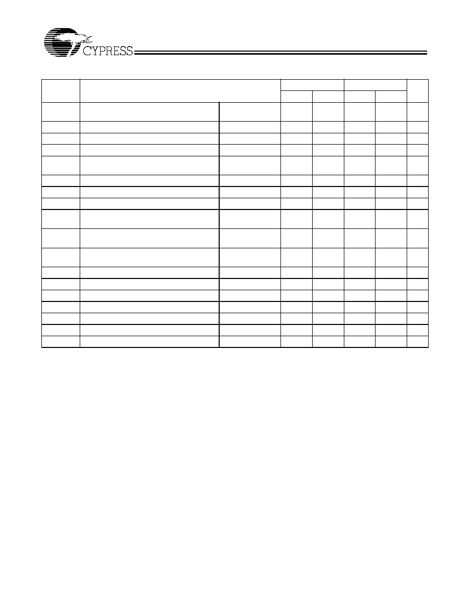
External Switching Characteristics
Over the Operating Range
Parameter
Description
7C341B-25
7C341B-35
Unit
Min.
Max
Min.
Max
t
PD1
Dedicated Input to Combinatorial Output
Delay
[4]
Commercial
25
35
ns
t
PD2
I/O Input to Combinatorial Output Delay
[4]
Commercial
40
55
ns
t
SU
Global Clock Set-up Time
Commercial
15
25
ns
t
CO1
Synchronous Clock Input to Output Delay
[4]
Commercial
14
20
ns
t
H
Input Hold Time from Synchronous Clock
Input
Commercial
0
0
ns
t
WH
Synchronous Clock Input High Time
Commercial
8
12.5
ns
t
WL
Synchronous Clock Input Low Time
Commercial
8
12.5
ns
f
MAX
Maximum Register Toggle Frequency
[5]
Commercial
62.5
40.0
MHz
t
ACO1
Dedicated Asynchronous Clock Input to
Output Delay
[4]
Commercial
25
35
ns
t
AS1
Dedicated Input or Feedback Set-up Time to
Asynchronous Clock Input
Commercial
5
10
ns
t
AH
Input Hold Time from Asynchronous Clock
Input
Commercial
6
10
ns
t
AWH
Asynchronous Clock Input HIGH Time
[6]
Commercial
11
16
ns
t
AWL
Asynchronous Clock Input LOW Time
[6]
Commercial
9
14
ns
t
CNT
Minimum Global Clock Period
Commercial
20
30
ns
t
ODH
Output Data Hold Time After Clock
Commercial
2
2
ns
f
CNT
Maximum Internal Global Clock Frequency
[7]
Commercial
50
33.3
MHz
t
ACNT
Minimum Internal Array Clock Frequency
Commercial
20
30
ns
f
ACNT
Maximum Internal Array Clock Frequency
[7]
Commercial
50
33.3
MHz
Notes:
4.
C1 = 35 pF.
5.
The f
MAX
values represent the highest frequency for pipeline data.
6.
This parameter is measured with a positive-edge-triggered clock at the register. For negative-edge clocking, the t
ACH
and t
ACL
parameter must be swapped.
7.
This parameter is measured with a 16-bit counter programmed into each LAB.