64-Macrocell MAXÆ EPLD
CY7C343B
Cypress Semiconductor Corporation
∑
3901 North First Street
∑
San Jose
∑
CA 95134
∑
408-943-2600
Document #: 38-03038 Rev. **
Revised December 8, 1999
43B
Features
∑ 64 MAX macrocells in 4 LABs
∑ 8 dedicated inputs, 24 bidirectional I/O pins
∑ Programmable interconnect array
∑ Advanced 0.65-micron CMOS technology to increase
performance
∑ Available in 44-pin HLCC, PLCC
∑ Lowest power MAX device
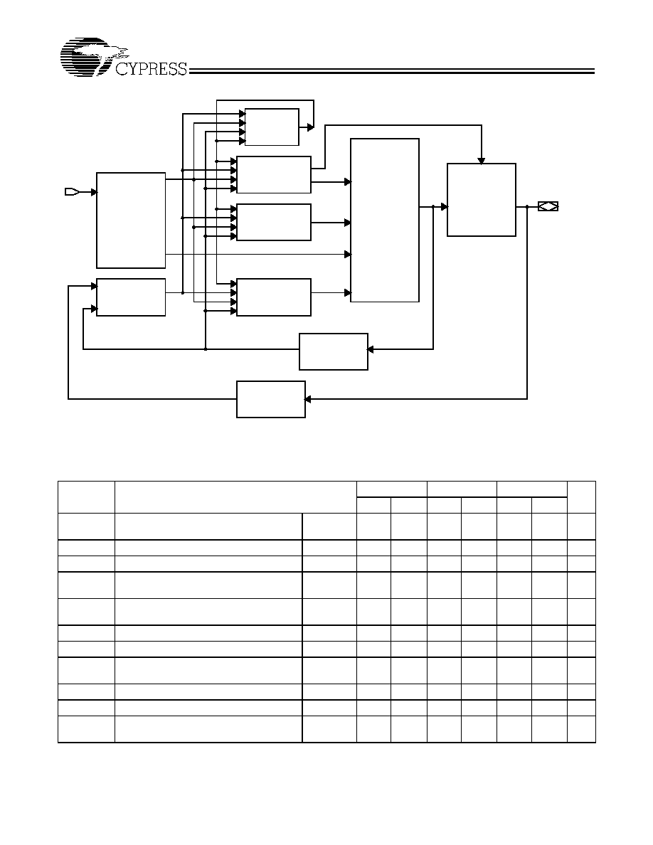
Functional Description
The CY7C343B is a high-performance, high-density erasable
programmable logic device, available in 44-pin PLCC and
HLCC packages.
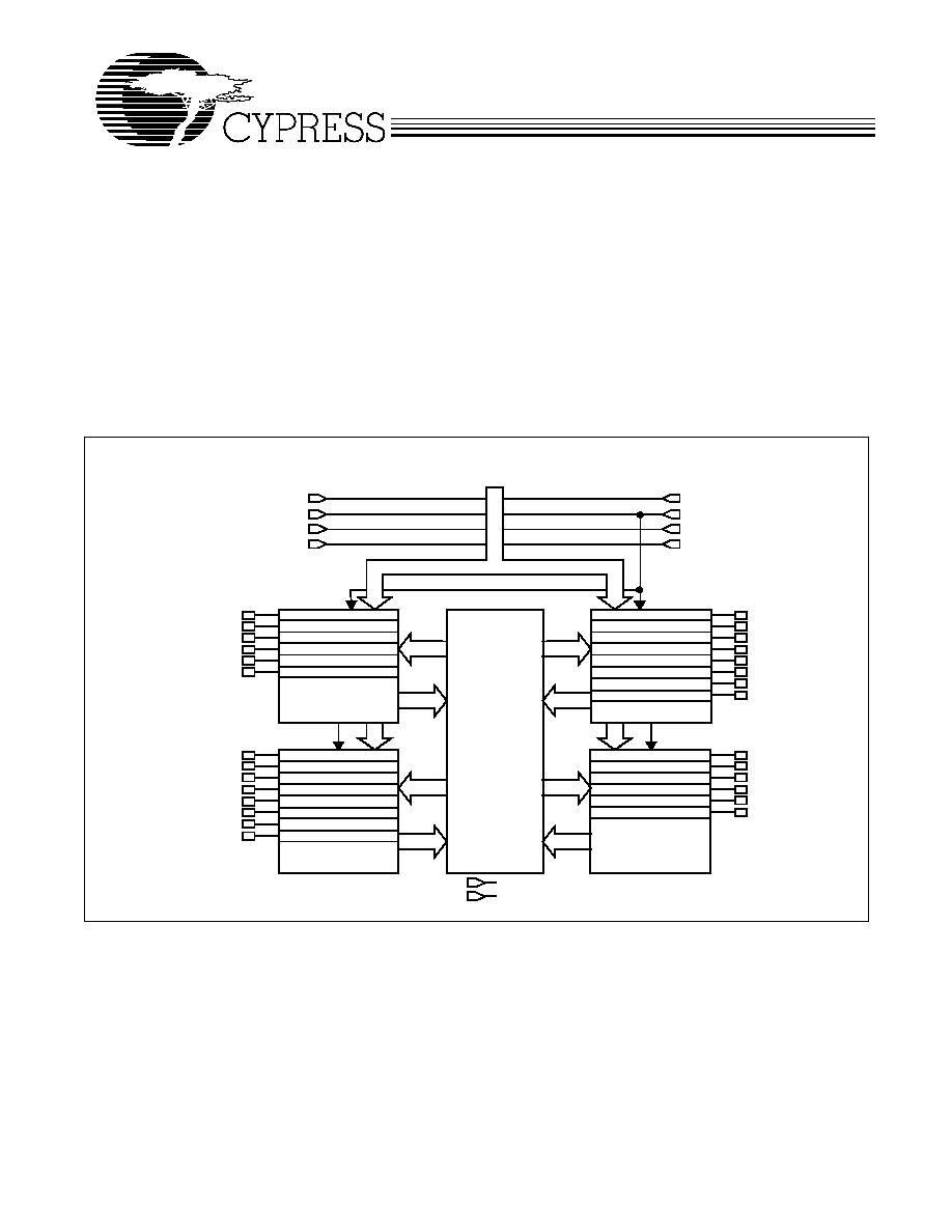
The CY7C343B contains 64 highly flexible macrocells and 128
expander product terms. These resources are divided into four
Logic Array Blocks (LABs) connected through the Program-
mable Inter-connect Array (PIA). There are 8 input pins, one
that doubles as a clock pin when needed. The CY7C343B also
has 28 I/O pins, each connected to a macrocell (6 for LABs A
and C, and 8 for LABs B and D). The remaining 36 macrocells
are used for embedded logic.
The CY7C343B is excellent for a wide range of both synchro-
nous and asynchronous applications.
MAX is a registered trademark of Altera Corporation.
MACROCELL 17
MACROCELL 18
MACROCELL 19
MACROCELL 20
MACROCELL 21
MACROCELL 22
MACROCELL 23
MACROCELL 24
MACROCELL 38
MACROCELL 37
MACROCELL 36
MACROCELL 35
MACROCELL 34
MACROCELL 33
9 INPUT
11 INPUT
12 INPUT
13 INPUT
P
I
A
MACROCELL 1
MACROCELL 2
MACROCELL 3
MACROCELL 4
MACROCELL 5
MACROCELL 6
MACROCELL 56
MACROCELL 55
MACROCELL 54
MACROCELL 53
MACROCELL 52
MACROCELL 51
MACROCELL 50
MACROCELL 49
MACROCELLS 7 - 16
MACROCELLS57 - 64
MACROCELLS 25 - 32
MACROCELLS39 - 48
INPUT 35
INPUT/CLK 34
INPUT 33
INPUT 31
2
4
5
6
7
8
1
44
42
41
40
39
38
37
30
29
28
27
26
24
SYSTEM CLOCK
(3, 14, 25, 36)
(10, 21, 32, 43)
V
CC
GND
LAB A
LAB B
LAB D
LAB C
C343B-1
Logic Block Diagram
DEDICATED INPUTS
I/O PINS
15
16
17
18
19
20
22
23
I/O PINS
I/O PINS
I/O PINS
CY7C343B
Document #: 38-03038 Rev. **
Page 2 of 12
Maximum Ratings
(Above which the useful life may be impaired. For user guide-
lines, not tested.)
Storage Temperature ..................................≠65∞C to+135∞C
Ambient Temperature with
Power Applied..............................................≠65∞C to+135∞C
Maximum Junction Temperature
(Under Bias)................................................................. 150∞C
Supply Voltage to Ground Potential
[1]
............. ≠2.0V to+7.0V
DC Output Current, per Pin
[1]
...................≠25 mA to +25 mA
DC Input Voltage
[1]
.........................................≠2.0V to +7.0V
Note:
1.
Minimum DC input is ≠0.3V. During transactions, the inputs may undershoot to ≠2.0V or overshoot to 7.0V for input currents less then 100 mA and periods
shorter than 20 ns.
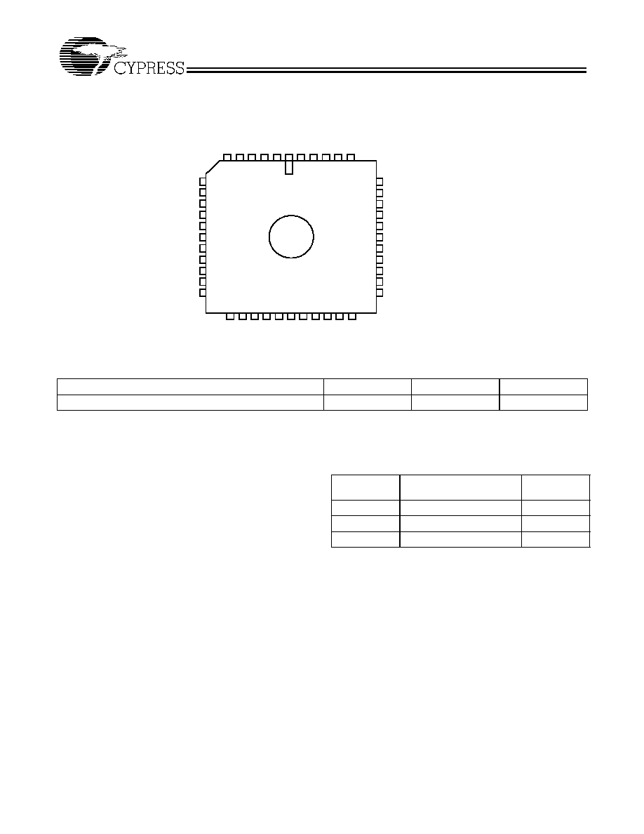
Pin Configuration
Selection Guide
7C343B-25
7C343B-30
7C343B-35
Maximum Access Time (ns)
25
30
35
I/O
4
5
3
10
11
9
8
7
36
35
37
38
39
19
18
20
12
13
34
33
2
1
21 22
HLCC, PLCC
Top View
17
16
15
14
23 24
26
25
27 28
29
30
31
32
44 43
41
42
40
V CC
GND
I/O
I/O
I/O
V
CC
INPUT
INPUT/CLK
INPUT
GND
INPUT
I/O
I/O
V CC
GND
I/O
C343B-2
6
7C343
I/O
I/O
I/O
I/O
I/O
I/O
I/O
I/O
INPUT
GND
V
CC
INPUT
INPUT
INPUT
I/O
I/O
I/O
I/O
I/O
I/O
I/O
I/O
I/O
I/O
I/O
I/O
I/O
Operating Range
Range
Ambient
Temperature
V
CC
Commercial
0∞C to +70
∞
C
5V
±
5%
Industrial
≠40
∞
C to +85
∞
C
5V
±
10%
Military
≠55
∞
C to +125
∞
C (Case)
5V
±
10%
CY7C343B
Document #: 38-03038 Rev. **
Page 3 of 12
Electrical Characteristics
Over the Operating Range
Parameter
Description
Test Conditions
Min.
Max.
Unit
V
CC
Supply Voltage
Maximum V
CC
rise time is 10 ms
4.75(4.5)
5.25(5.5)
V
V
OH
Output HIGH Voltage
I
OH
= ≠4.0 mA DC
[2]
2.4
V
V
OL
Output LOW Voltage
I
OL
= 8 mA DC
[2]
0.45
V
V
IH
Input HIGH Level
2.0
V
CC
+0.3
V
V
IL
Input LOW Level
≠0.3
0.8
V
I
IX
Input Current
V
I
= V
CC
or ground
≠10
+10
µ
A
I
OZ
Output Leakage Current
V
O
= V
CC
or ground
≠40
+40
µ
A
t
R
Recommended Input Rise Time
100
ns
t
F
Recommended Input Fall Time
100
ns
Capacitance
Parameter
Description
Test Conditions
Max.
Unit
C
IN
Input Capacitance
V
IN
= 0V, f = 1.0 MHz
10
pF
C
OUT
Output Capacitance
V
OUT
= 0V, f = 1.0 MHz
20
pF
Note:
2.
The I
OH
parameter refers to high-level TTL output current; the I
OL
parameter refers to low-level TTL output current.
AC Test Loads and Waveforms
3.0V
5V
OUTPUT
R1 464
R2
250
50 pF
INCLUDING
JIG AND
SCOPE
GND
90%
10%
90%
10%
<6 ns
5V
OUTPUT
R1 464
R2
250
5 pF
INCLUDING
JIG AND
SCOPE
(a)
(b)
OUTPUT
1.75V
Equivalent to:
TH…
VENIN EQUIVALENT (commercial/military)
ALL INPUT PULSES
C343B-4
C343B-5
163
<6 ns
CY7C343B
Document #: 38-03038 Rev. **
Page 4 of 12
Programmable Interconnect Array
The Programmable Interconnect Array (PIA) solves intercon-
nect limitations by routing only the signals needed by each
logic array block. The inputs to the PIA are the outputs of every
macrocell within the device and the I/O pin feedback of every
pin on the device.
Unlike masked or programmable gate arrays, which induce
variable delay dependent on routing, the PIA has a fixed delay.
This eliminates undesired skews among logic signals, which
may cause glitches in internal or external logic. The fixed de-
lay, regardless of programmable interconnect array configura-
tion, simplifies design by ensuring that internal signal skews or
races are avoided. The result is simpler design implementa-
tion, often in a single pass, without the multiple internal logic
placement and routing iterations required for a programmable
gate array to achieve design timing objectives.
Design Recommendations
Operation of the devices described herein with conditions
above those listed under "Absolute Maximum Ratings" may
cause permanent damage to the device. This is a stress rating
only and functional operation of the device at these or any
other conditions above those indicated in the operational sec-
tions of this data sheet is not implied. Exposure to absolute
maximum ratings conditions for extended periods of time may
affect device reliability. The CY7C343B contains circuitry to
protect device pins from high static voltages or electric fields;
however, normal precautions should be taken to avoid apply-
ing any voltage higher than maximum rated voltages.
For proper operation, input and output pins must be con-
strained to the range GND < (V
IN
or V
OUT
) < V
CC
. Unused
inputs must always be tied to an appropriate logic level (either
V
CC
or GND). Each set of V
CC
and GND pins must be con-
nected together directly at the device. Power supply decou-
pling capacitors of at least 0.2
µ
F must be connected between
V
CC
and GND. For the most effective decoupling, each V
CC
pin should be separately decoupled to GND, directly at the
device. Decoupling capacitors should have good frequency
response, such as monolithic ceramic types.
Timing Considerations
Unless otherwise stated, propagation delays do not include
expanders. When using expanders, add the maximum ex-
pander delay t
EXP
to the overall delay. Similarly, there is an
additional t
PIA
delay for an input from an I/O pin when com-
pared to a signal from a straight input pin.
When calculating synchronous frequencies, use t
S1
if all inputs
are on the input pins. When expander logic is used in the data
path, add the appropriate maximum expander delay, t
EXP
to
t
S1
. Determine which of 1/(t
WH
+ t
WL
), 1/t
CO1
, or 1/(t
EXP
+ t
S1
)
is the lowest frequency. The lowest of these frequencies is the
maximum data path frequency for the synchronous configura-
tion.
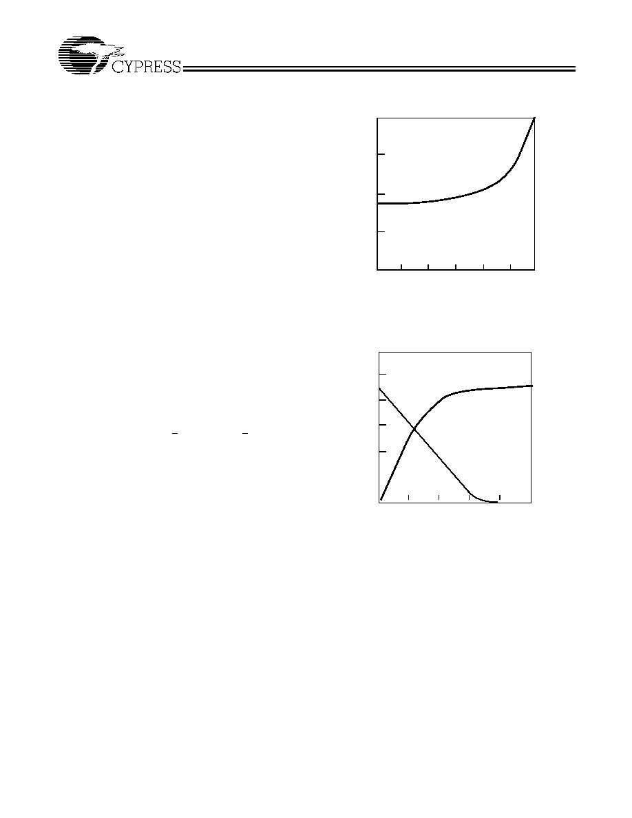
Typical I
CC
vs. f
MAX
Output Drive Current
When calculating external asynchronous frequencies, use
t
AS1
if all inputs are on dedicated input pins.
When expander logic is used in the data path, add the appro-
priate maximum expander delay, t
EXP
to t
AS1
. Determine
which of 1/(t
AWH
+ t
AWL
), 1/t
ACO1
, or 1/(t
EXP
+ t
AS1
) is the low-
est frequency. The lowest of these frequencies is the maxi-
mum data path frequency for the asynchronous configuration.
The parameter t
OH
indicates the system compatibility of this
device when driving other synchronous logic with positive in-
put hold times, which is controlled by the same synchronous
clock. If t
OH
is greater than the minimum required input hold
time of the subsequent synchronous logic, then the devices
are guaranteed to function properly with a common synchro-
nous clock under worst-case environmental and supply volt-
age conditions.
200
150
100
50
1 kHz
10 kHz
100 kHz
1 MHz
I
CC
MAXIMUM FREQUENCY
10 MHz
0
50 MHz
100 Hz
ACT
I
V
E
(mA
) T
y
p.
V
CC
= 5.0V
Room Temp.
C343B≠7
0
1
2
3
4
I
OUT
P
UT CUR
RE
NT (
m
A
)
TY
P
I
C
A
L
V
O
OUTPUT VOLTAGE (V)
250
200
150
100
50
5
O
I
OH
I
OL
V
CC
= 5.0V
Room Temp.
C343B≠8
CY7C343B
Document #: 38-03038 Rev. **
Page 5 of 12
Figure 1. CY7C343B Internal Timing Model
External Synchronous Switching Characteristics
Over Operating Range
Parameter
Description
7C343B-25
7C343B-30
7C343B-35
Unit
Min.
Max.
Min.
Max.
Min.
Max.
t
PD1
Dedicated Input to Combinatorial Output
Delay
[3]
Com'l/Ind
25
30
35
ns
t
PD2
I/O Input to Combinatorial Output Delay
[3]
Com'l/Ind
40
45
55
ns
t
SU
Global clock setup time
Com'l/ Ind
15
20
25
ns
t
CO1
Synchronous Clock Input to Output
Delay
[3]
Com'l/Ind
14
16
20
ns
t
H
Input Hold Time from Synchronous Clock
Input
Com'l/Ind
0
0
0
ns
t
WH
Synchronous Clock Input HIGH Time
Com'l/Ind
8
10
12.5
ns
t
WL
Synchronous Clock Input LOW Time
Com'l/Ind
8
10
12.5
ns
f
MAX
Maximum Register Toggle Frequency
[4]
Com'l/Ind
62.5
50
40
MH
z
t
CNT
Minimum Global Clock Period
Com'l/Ind
20
25
30
ns
t
ODH
Output Data Hold Time After Clock
Com'l/Ind
2
2
2
ns
f
CNT
Maximum Internal Global Clock
Frequency
[5]
Com'l/Ind
50
40
33.3
MH
z
Notes:
3.
C1 = 35 pF.
4.
The f
MAX
values represent the highest frequency for pipeline data.
5.
This parameter is measured with a 16-bit counter programmed into each LAB.
LOGIC ARRAY
CONTROL DELAY
t
LAC
EXPANDER
DELAY
t
EXP
CLOCK
DELAY
t
IC
t
RD
t
COMB
t
LATCH
INPUT
DELAY
t
IN
PIA
DELAY
t
PIA
REGISTER
OUTPUT
DELAY
t
OD
t
XZ
t
ZX
LOGIC ARRAY
DELAY
t
LAD
FEEDBACK
DELAY
t
FD
I/O DELAY
t
IO
INPUT/
OUTPUT
INPUT
C343B-9
SYSTEM CLOCK DELAY t
ICS
t
RH
t
RSU
t
PRE
t
CLR