UltraLogicTM 64-Macrocell Flash CPLD
CY7C372i
Cypress Semiconductor Corporation
∑
3901 North First Street
∑
San Jose
∑
CA 95134
∑
408-943-2600
Document #: 38-03033 Rev. **
Revised July 10, 2000
72i
Features
∑ 64 macrocells in four logic blocks
∑ 32 I/O pins
∑ 5 dedicated inputs including 2 clock pins
∑ In-System Reprogrammable (ISRTM) Flash technology
-- JTAG interface
∑ Bus Hold capabilities on all I/Os and dedicated inputs
∑ No hidden delays
∑ High speed
-- f
MAX
= 125 MHz
-- t
PD
= 10 ns
-- t
S
= 5.5 ns
-- t
CO
= 6.5 ns
∑ Fully PCI compliant
∑ 3.3V or 5.0V I/O operation
∑ Available in 44-pin PLCC, TQFP, and CLCC packages
∑ Pin compatible with the CY7C371i
Functional Description
The CY7C372i is an In-System Reprogrammable Complex
Programmable Logic Device (CPLD) and is part of the
F
LASH
370iTM family of high-density, high-speed CPLDs. Like
all members of the F
LASH
370i family, the CY7C372i is de-
signed to bring the ease of use and high performance of the
22V10, as well as PCI Local Bus Specification support, to
high-density CPLDs.
Like all of the UltraLogicTM F
LASH
370i devices, the CY7C372i
is electrically erasable and In-System Reprogrammable (ISR),
which simplifies both design and manufacturing flows, thereby
reducing costs. The Cypress ISR function is implemented
through a JTAG serial interface. Data is shifted in and out
through the SDI and SDO pins. The ISR interface is enabled
using the programming voltage pin (ISR
EN
). Additionally, be-
cause of the superior routability of the F
LASH
370i devices, ISR
often allows users to change existing logic designs while si-
multaneously fixing pinout assignments.
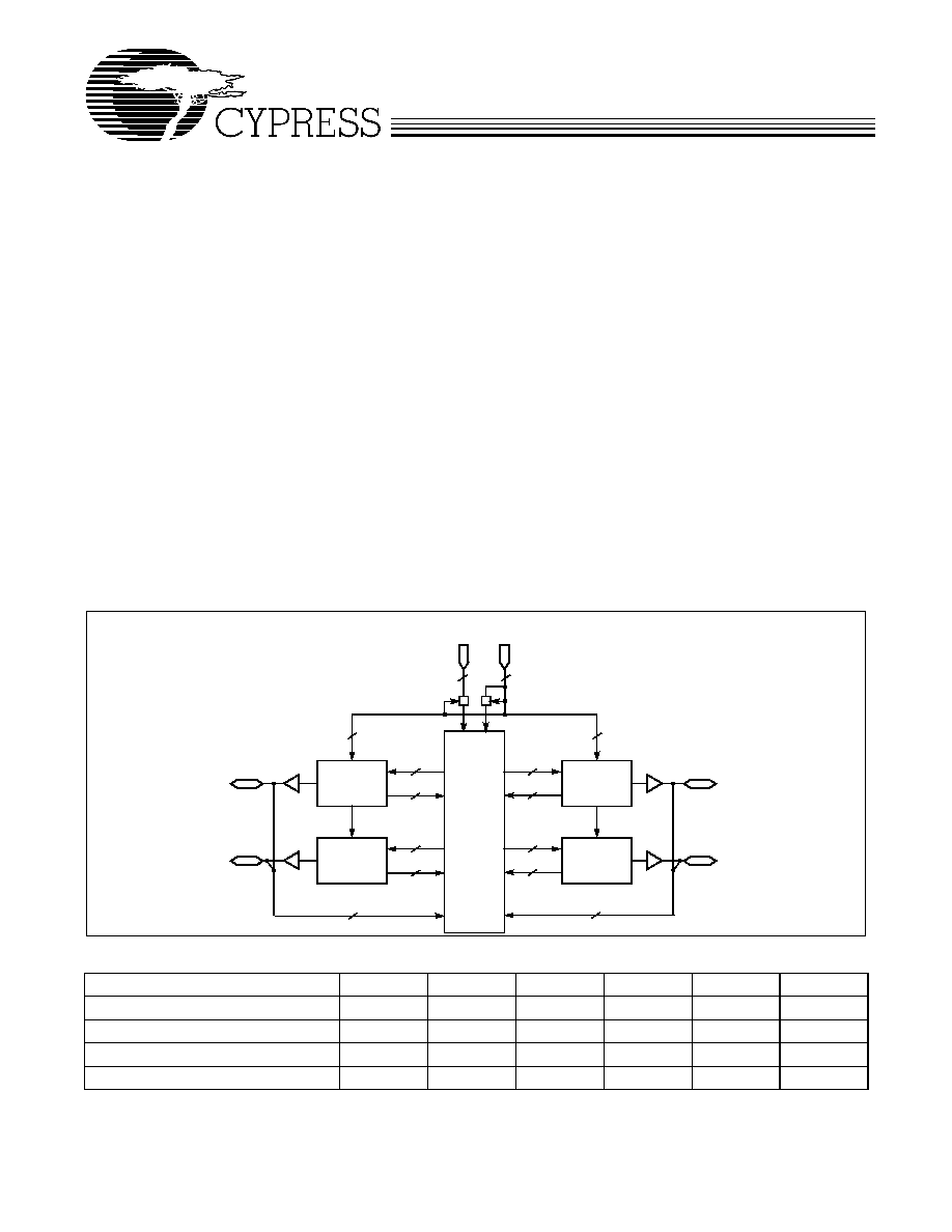
The 64 macrocells in the CY7C372i are divided between four
logic blocks. Each logic block includes 16 macrocells, a
72 x 86 product term array, and an intelligent product term al-
locator.
The logic blocks in the F
LASH
370i architecture are connected
with an extremely fast and predictable routing resource--the
Programmable Interconnect Matrix (PIM). The PIM brings flex-
ibility, routability, speed, and a uniform delay to the intercon-
nect.
Logic Block Diagram
7c372i≠1
PIM
INPUT
MACROCELLS
CLOCK
INPUTS
INPUTS
LOGIC
LOGIC
2
2
36
16
16
36
8 I/Os
8 I/Os
16
16
LOGIC
36
16
16
36
8 I/Os
8 I/Os
2
3
INPUT/CLOCK
MACROCELLS
I/O
0
-I/O
7
LOGIC
I/O
8
-I/O
15
I/O
16
-I/O
23
I/O
24
-I/O
31
BLOCK
A
BLOCK
B
BLOCK
D
BLOCK
C
Selection Guide
7C372i-125
7C372i-100
7C372i-83
7C372iL-83
7C372i-66
7C372iL-66
Maximum Propagation Delay
[1]
, t
PD
(ns)
10
12
15
15
20
20
Minimum Set-up, t
S
(ns)
5.5
6.0
8
8
10
10
Maximum Clock to Output
[1]
, t
CO
(ns)
6.5
6.5
8
8
10
10
Typical Supply Current, I
CC
(mA)
75
75
75
45
75
45
Note:
1.
The 3.3V I/O mode timing adder, t
3.3IO
, must be added to this specification when V
CCIO
= 3.3V.

CY7C372i
Document #: 38-03033 Rev. **
Page 2 of 12
Functional Description
(continued)
Like all members of the F
LASH
370i family, the CY7C372i is rich
in I/O resources. Every two macrocells in the device feature an
associated I/O pin, resulting in 32 I/O pins on the CY7C372i.
In addition, there are three dedicated inputs and two in-
put/clock pins.
Finally, the CY7C372i features a very simple timing model.
Unlike other high-density CPLD architectures, there are no
hidden speed delays such as fanout effects, interconnect de-
lays, or expander delays. Regardless of the number of re-
sources used. or the type of application, the timing parameters
on the CY7C372i remain the same.
Logic Block
The number of logic blocks distinguishes the members of the
F
LASH
370i family. The CY7C372i includes four logic blocks.
Each logic block is constructed of a product term array, a prod-
uct term allocator, and 16 macrocells.
Product Term Array
The product term array in the F
LASH
370i logic block includes
36 inputs from the PIM and outputs 86 product terms to the
product term allocator. The 36 inputs from the PIM are avail-
able in both positive and negative polarity, making the overall
array size 72 x 86. This large array in each logic block allows
for very complex functions to be implemented in a single pass
through the device.
Product Term Allocator
The product term allocator is a dynamic, configurable resource
that shifts product terms to macrocells that require them. Any
number of product terms between 0 and 16 inclusive can be
assigned to any of the logic block macrocells (this is called
product term steering). Furthermore, product terms can be
shared among multiple macrocells. This means that product
terms that are common to more than one output can be imple-
mented in a single product term. Product term steering and
product term sharing help to increase the effective density of
the F
LASH
370 PLDs. Note that product term allocation is han-
dled by software and is invisible to the user.
I/O Macrocell
Half of the macrocells on the CY7C372i have separate I/O pins
associated with them. In other words, each I/O pin is shared
by two macrocells. The input to the macrocell is the sum of
between 0 and 16 product terms from the product term alloca-
tor. The macrocell includes a register that can be optionally
bypassed. It also has polarity control, and two global clocks to
trigger the register. The I/O macrocell also features a separate
feedback path to the PIM so that the register can be buried if
the I/O pin is used as an input.
Buried Macrocell
The buried macrocell is very similar to the I/O macrocell.
Again, it includes a register that can be configured as combi-
natorial, as a D flip-flop, a T flip-flop, or a latch. The clock for
this register has the same options as described for the I/O
macrocell. One difference on the buried macrocell is the addi-
tion of input register capability. The user can program the bur-
ied macrocell to act as an input register (D-type or latch)
whose input comes from the I/O pin associated with the neigh-
boring macrocell. The output of all buried macrocells is sent
directly to the PIM regardless of its configuration.
Programmable Interconnect Matrix
The Programmable Interconnect Matrix (PIM) connects the
four logic blocks on the CY7C372i to the inputs and to each
other. All inputs (including feedbacks) travel through the PIM.
There is no speed penalty incurred by signals traversing the
PIM.
Programming
For an overview of ISR programming, refer to the F
LASH
370i
Family data sheet and for ISR cable and software specifica-
tions, refer to ISR data sheets. For a detailed description of
ISR capabilities, refer to the Cypress application note, "An In-
troduction to In System Reprogramming with F
LASH
370i."
Pin Configurations
7c372i-2
I/O
27
/SDI
I/O
26
I/O
25
I/O
24
CLK
1
/I
4
GND
I
3
I
2
I/O
23
I/O
22
I/O
21
I/O
5
/SCLK
I/O
6
I/O
7
I
0
ISR
EN
GND
CLK
0
/I
1
I/O
8
I/O
9
I/O
10
I/O
11
GND
I/O
20
I/O
2
GND
V
CCIO
V
CCINT
I/O
3
I/O
4
I/O
1
I/O
0
I/O
29
I/O
30
I/O
31
I/O
28
I/O
19
I/O
18
I/O
17
I/O
16
I/O
15
I/O
14
I/O
13
I/O
12
6 5
3
4
2
8
9
7
10
11
1 44
18
15
16
14
13
12
17
19 20
22
21
23 24
27
26
28
25
31
30
29
32
33
34
39
37
38
36
35
43 42
40
41
PLCC
TopView
/S
MODE
/S
DO
7c372i≠4
1
7
8
9
10
11
12
13
14
15
16
17
39
38
37
36
35
34
33
32
31
30
29
18 19 20 21 22 23 24 25 26 27 28
6 5 4 3 2
44 43 42 41 40
I/O
27
/SDI
I/O
26
I/O
25
I/O
24
CLK
1
/I
4
GND
I
3
I
2
I/O
23
I/O
22
I/O
21
I/O
5
/SCLK
I/O
6
I/O
7
I
0
ISR
EN
GND
CLK
0
/I
1
I/O
8
I/O
9
I/O
10
I/O
11
GND
I/O
20
I/O
2
GND
V
CC
V
CC
I/O
3
I/O
4
I/O
1
I/O
0
I/O
29
I/O
30
I/O
31
I/O
28
I/O
19
I/O
18
I/O
17
I/O
16
I/O
15
I/O
14
I/O
13
I/O
12
/S
MODE
/S
DO
CLCC
TopView
CY7C372i
Document #: 38-03033 Rev. **
Page 3 of 12
PCI Compliance
The F
LASH
370i family of CMOS CPLDs are fully compliant with
the PCI Local Bus Specification published by the PCI Special
Interest Group. The simple and predictable timing model of
F
LASH
370i ensures compliance with the PCI AC specifications
independent of the design. On the other hand, in CPLD and
FPGA architectures without simple and predictable timing, PCI
compliance is dependent upon routing and product term dis-
tribution.
3.3V or 5.0V I/O operation
The F
LASH
370i family can be configured to operate in both
3.3V and 5.0V systems. All devices have two sets of V
CC
pins:
one set, V
CCINT
, for internal operation and input buffers, and
another set, V
CCIO
, for I/O output drivers. V
CCINT
pins must
always be connected to a 5.0V power supply. However, the
V
CCIO
pins may be connected to either a 3.3V or 5.0V power
supply, depending on the output requirements. When V
CCIO
pins are connected to a 5.0V source, the I/O voltage levels are
compatible with 5.0V systems. When V
CCIO
pins are connect-
ed to a 3.3V source, the input voltage levels are compatible
with both 5.0V and 3.3V systems, while the output voltage lev-
els are compatible with 3.3V systems. There will be an addi-
tional timing delay on all output buffers when operating in 3.3V
I/O mode. The added flexibility of 3.3V I/O capability is avail-
able in commercial and industrial temperature ranges.
Bus Hold Capabilities on all I/Os and Dedicated Inputs
In addition to ISR capability, a new feature called bus-hold has
been added to all F
LASH
370i I/Os and dedicated input pins.
Bus-hold, which is an improved version of the popular internal
pull-up resistor, is a weak latch connected to the pin that does
not degrade the device's performance. As a latch, bus-hold
recalls the last state of a pin when it is three-stated, thus re-
ducing system noise in bus-interface applications. Bus-hold
additionally allows unused device pins to remain unconnected
on the board, which is particularly useful during prototyping as
designers can route new signals to the device without cutting
trace connections to V
CC
or GND.
Design Tools
Development software for the CY7C372i is available from
Cypress's WarpTM, Warp ProfessionalTM, and Warp Enter-
priseTM software packages. Please refer to the data sheets on
these products for more details. Cypress also actively sup-
ports almost all third-party design tools. Please refer to
third-party tool support for further information.
Maximum Ratings
(Above which the useful life may be impaired. For user guide-
lines, not tested.)
Storage Temperature ................................. ≠65
∞
C to +150
∞
C
Ambient Temperature with
Power Applied ............................................ ≠55
∞
C to +125
∞
C
Supply Voltage to Ground Potential ...............≠0.5V to +7.0V
DC Voltage Applied to Outputs
in High Z State................................................≠0.5V to +7.0V
DC Input Voltage ............................................≠0.5V to +7.0V
DC Program Voltage .................................................... 12.5V
Output Current into Outputs ........................................ 16 mA
Static Discharge Voltage ........................................... >2001V
(per MIL≠STD≠883, Method 3015)
Latch-Up Current ..................................................... >200 mA
Note:
2.
T
A
is the "instant on" case temperature.
Operating Range
Range
Ambient
Temperature
V
CC
V
CCINT
V
CCIO
Commercial
0
∞
C to +70
∞
C
5V
±
0.25V
5V
±
0.25V
OR
3.3V
±
0.3V
Industrial
-
40
∞
C to +85
∞
C
5V
±
0.5V
5V
±
0.5V
OR
3.3V
±
0.3V
Military
[2]
≠55∞C to +125∞C
5V
±
0.5V
CY7C372i
Document #: 38-03033 Rev. **
Page 4 of 12
Notes:
3.
See the last page of this specification for Group A subgroup testing information.
4.
If V
CCIO
is not specified, the device can be operating in either 3.3V or 5V I/O mode; V
CC
=V
CCINT
.
5.
For SDO: I
OH
=≠2 mA, I
OL
= 2 mA.
6.
When the I/O is three-stated, the bus-hold circuit can weakly pull the I/O to a maximum of 4.0V if no leakage current is allowed. This voltage is lowered significantly
by a small leakage current. Note that all I/Os are three-stated during ISR programming. Refer to the application note "Understanding Bus Hold" for additional
information.
7.
These are absolute values with respect to device ground. All overshoots due to system or tester noise are included.
8.
Not more than one output should be tested at a time. Duration of the short circuit should not exceed 1 second. V
OUT
= 0.5V has been chosen to avoid test
problems caused by tester ground degradation.
9.
Tested initially and after any design or process changes that may affect these parameters.
10. Measured with 16-bit counter programmed into each logic block.
11. C
I/O
for dedicated Inputs, and for I/O pins with JTAG functionality is 12 pF Max., and for ISR
EN
is 15pF Max.
12. C
I/O
for CLCC package is 15 pF Max.
Electrical Characteristics
Over the Operating Range
[
3, 4]
Parameter
Description
Test Conditions
Min.
Typ.
Max.
Unit
V
OH
Output HIGH Voltage
V
CC
= Min.
I
OH
= ≠3.2 mA (Com'l/Ind)
[5]
2.4
V
I
OH
= ≠2.0 mA (Mil)
2.4
V
V
OHZ
Output HIGH Voltage with
Output Disabled
[8]
V
CC
= Max. I
OH
= 0
µ
A (Com'l/Ind)
[5, 6]
4.0
V
I
OH
= ≠50
µ
A (Com'l/Ind)
[5, 6]
3.6
V
V
OL
Output LOW Voltage
V
CC
= Min.
I
OL
= 16 mA (Com'l/Ind)
[5]
0.5
V
I
OL
= 12 mA (Mil)
0.5
V
V
IH
Input HIGH Voltage
Guaranteed Input Logical HIGH Voltage for all
Inputs
[7]
2.0
7.0
V
V
IL
Input LOW Voltage
Guaranteed Input Logical LOW Voltage for all
Inputs
[7]
≠0.5
0.8
V
I
IX
Input Load Current
V
I
= Internal GND, V
I
= V
CC
≠10
+10
µ
A
I
OZ
Output Leakage Current
V
CC
= Max., V
O
= GND or V
O
= V
CC
, Output
Disabled
≠50
+50
µ
A
V
CC
= Max., V
O
= 3.3V, Output Disabled
[6]
0
≠70
≠125
µ
A
I
OS
Output Short
Circuit Current
[8, 9]
V
CC
= Max., V
OUT
= 0.5V
≠30
≠160
mA
I
CC
Power Supply Current
[10]
V
CC
= Max., I
OUT
= 0 mA,
f = 1 MHz, V
IN
= GND, V
CC
Com'l/Ind.
75
125
mA
Com'l "L" ≠66
45
75
mA
Military
75
200
mA
I
BHL
Input Bus Hold LOW
Sustaining Current
V
CC
= Min., V
IL
= 0.8V
+75
µ
A
I
BHH
Input Bus Hold HIGH
Sustaining Current
V
CC
= Min., V
IH
= 2.0V
≠75
µ
A
I
BHLO
Input Bus Hold LOW
Overdrive Current
V
CC
= Max.
+500
µ
A
I
BHHO
Input Bus Hold HIGH
Overdrive Current
V
CC
= Max.
-
500
µ
A
Capacitance
[
9]
Parameter
Description
Test Conditions
Min.
Max.
Unit
C
I/O
[11, 12]
Input Capacitance
V
IN
= 5.0V at f = 1 MHz
8
pF
C
CLK
Clock Signal Capacitance
V
IN
= 5.0V at f = 1 MHz
5
12
pF
Inductance
[
9]
Parameter
Description
Test Conditions
44-Lead CLCC
44-Lead PLCC
Unit
L
Maximum Pin Inductance
V
IN
= 5.0V at f = 1 MHz
2
5
nH
CY7C372i
Document #: 38-03033 Rev. **
Page 5 of 12
Note:
13. t
ER
measured with 5-pF AC Test Load and t
EA
measured with 35-pF AC Test Load.
Endurance Characteristics
[
9]
Parameter
Description
Test Conditions
Max.
Unit
N
Maximum Reprogramming Cycles
Normal Programming Conditions
100
Cycles
AC Test Loads and Waveforms
7c372i≠3
7c372i≠4
90%
10%
3.0V
GND
90%
10%
ALL INPUT PULSES
5V
OUTPUT
35 pF
INCLUDING
JIG AND
SCOPE
5V
OUTPUT
5 pF
INCLUDING
JIG AND
SCOPE
(a)
(b)
< 2 ns
< 2 ns
OUTPUT
238
(com'l)
319
(mil)
170
(com'l)
236
(mil)
99
(com'l)
136
(mil)
Equivalent to:
TH… VENIN EQUIVALENT
2.08V(com'l)
2.13V(mil)
238
(com'l)
319
(mil)
170
(com'l)
236
(mil)
(c)
Parameter
[13]
V
x
Output Waveform Measurement Level
t
ER(≠)
1.5V
t
ER(+)
2.6V
t
EA(+)
1.5V
t
EA(≠)
V
the
(d) Test Waveforms
V
OH
0.5V
V
X
0.5V
V
OL
V
X
0.5V
V
X
V
OH
0.5V
V
X
V
OL