64 x 8 Cascadable FIFO
64 x 9 Cascadable FIFO
CY7C408A
CY7C409A
Cypress Semiconductor Corporation
∑
3901 North First Street
∑
San Jose
∑
CA 95134
∑
408-943-2600
July 1986 ≠ Revised July 1994
1CY 7C40 9A
Features
∑ 64 x 8 and 64 x 9 first-in first-out (FIFO) buffer memory
∑ 35-MHz shift in and shift out rates
∑ Almost Full/Almost Empty and Half Full flags
∑ Dual-port RAM architecture
∑ Fast (50-ns) bubble-through
∑ Independent asynchronous inputs and outputs
∑ Output enable (CY7C408A)
∑ Expandable in word width and FIFO depth
∑ 5V
±
10% supply
∑ TTL complete
∑ Capable of withstanding greater than 2001V electro-
static discharge voltage
∑ 300-mil, 28-pin DIP
Functional Description
The CY7C408A and CY7C409A are 64-word deep by 8- or
9-bit wide first-in first-out (FIFO) buffer memories. In addition
to the industry-standard handshaking signals, almost full/al-
most empty (AFE) and half-full (HF) flags are provided.
AFE is HIGH when the FIFO is almost full or almost empty,
otherwise AFE is LOW. HF is HIGH when the FIFO is half full,
otherwise HF is LOW.
The CY7C408A has an output enable (OE) function.
The memory accepts 8- or 9-bit parallel words as its inputs (DI
0
≠ DI
8
) under the control of the shift in (SI) input when the input
ready (IR) control signal is HIGH. The data is output, in the
same order as it was stored on the DO
0
≠ DO
8
output pins
under the control of the shift out (SO) input when the output
ready (OR) control signal is HIGH. If the FIFO is full (IR LOW),
pulses at the SI input are ignored; if the FIFO is empty (OR
LOW), pulses at the SO input are ignored.
The IR and OR signals are also used to connect the FIFOs in
parallel to make a wider word or in series to make a deeper
buffer, or both.
Parallel expansion for wider words is implemented by logically
ANDing the IR an OR outputs (respectively) of the individual
FIFOs together (
Figure 5). The AND operation insures that all
of the FIFOs are either ready to accept more data (IR HIGH)
or ready to output data (OR HIGH) and thus compensate for
variations in propagation delay times between devices.
Serial expansion (cascading) for deeper buffer memories is
accomplished by connecting data outputs of the FIFO closet
to the data source (upstream device) to the data inputs of the
following (downstream) FIFO (
Figure 4). In addition, to insure
proper operation, the SO signal of the upstream FIFO must be
connected to the OR output of the upstream FIFO. In this serial
expansion configuration, the IR and OR signals are used to
pass data through the FIFOs.
Reading and writing operations are completely asynchronous,
allowing the FIFO to be used as a buffer between two digital
machines of widely differing operating frequencies. The high
shift in and shift out rates of these FIFOs, and their throughput
rate due to the fast bubblethrough time, which is due to their
dual-port RAM architecture, make them ideal for high-speed
communications and controllers.
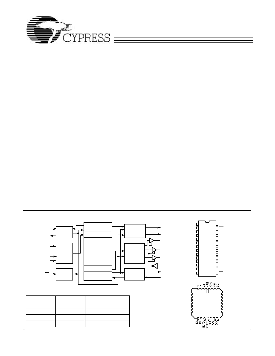
Logic Block Diagram
Pin Configurations
C408A≠1
INPUT
CONTROL
LOGIC
SI
IR
DATA IN
DI0
DI 7
(7C409A)DI8
MASTER
RESET
MR
WRITE MULTIPLEXER
WRITE POINTER
READ MULTIPLEXER
READ POINTER
MEMORY
ARRAY
OUTPUT
CONTROL
LOGIC
DATA OUT
ALMOST FULL/
ALMOST EMPTY
HALF FULL
OE (7C408A)
DO0
DO7
DO8 (7C409A)
SO
OR
.
.
.
.
.
.
HF
AFE
1
2
3
4
5
6
7
8
9
10
11
12
15
16
17
18
19
20
24
23
22
21
13
14
25
28
27
26
AFE
HF
IR
SI
DI 0
DI 1
GND
DI 2
DI 3
DI 4
(7C408A) NC
(7C409A) DI8
VCC
MR
SO
OR
DO0
DO1
GND
DO2
DO3
DO4
DO5
DO7
DO6
OE (7C408A)
DO8 (7C409A)
C408A≠2
C408A≠3
27
4
5
6
7
8
9
10
3 2 1
26
12 13 14 15
22
21
20
19
11
1617 18
23
24
25
28
OR
DO 0
DO 1
GND
DO 2
DO 3
DO 4
DI 0
DI 1
GND
DI 2
DI 3
DI 4
DI 5
7C408A
7C409A
7C408A
7C409A
DI 5
DI 6
DI 7
Flag Definitions
HF
AFE
Words Stored
L
H
0 - 8
L
L
9 - 31
H
L
32 - 55
H
H
56 - 64
CY7C408A
CY7C409A
2
Maximum Ratings
(Above which the useful life may be impaired. For user guide-
lines, not tested.)
Storage Temperature
..................................... -
65
∞
C to +150
∞
C
Ambient Temperature with
Power Applied
.................................................. -
55
∞
C to +125
∞
C
Supply Voltage to Ground Potential
.................-
0.5V to +7.0V
DC Voltage Applied to Outputs
in High Z State (7C408A)
...................................-
0.5V to +7.0V
DC Input Voltage
.................................................-
3.0V to +7.0V
Power Dissipation.......................................................... 1.0W
Output Current, into Outputs (Low) ............................. 20 mA
Static Discharge Voltage ........................................... >2001V
(per MIL-STD-883, Method 3015)
Selection Guide
7C408A-15
7C409A-15
7C408A-25
7C409A-25
7C408A-35
7C409A-35
Maximum Shift Rate (MHz)
15
25
35
Maximum Operating
Current (mA)
[1]
Commercial
115
125
135
Military
140
150
N/A
Operating Range
Range
Ambient
Temperature
V
CC
Commercial
0
∞
C to +70
∞
C 5V
±
10%
Military
[2]
-
55
∞
C to +125
∞
C 5V
±
10%
Electrical Characteristics
Over the Operating Range (Unless Otherwise Noted)
[3]
Parameter
Description
Test Conditions
Min.
Max.
Unit
V
OH
Output HIGH Voltage
V
CC
= Min., I
OH
= ≠4.0 mA
2.4
V
V
OL
Output LOW Voltage
V
CC
= Min., I
OL
= 8.0 mA
0.4
V
V
IH
Input HIGH Voltage
2.2
V
CC
V
V
IL
Input LOW Voltage
-
3.0
0.8
V
I
IX
Input Leakage Current
GND < V
I
< V
CC
-
10
+10
µ
A
I
OS
Output Short Circuit Current
[4]
V
CC
= Max., V
OUT
= GND
-
90
mA
I
CCQ
Quiescent Power Supply Current
V
CC
= Max., I
OUT
= 0 mA
V
IN
< V
IL
, V
IN
> V
IH
Commercial
100
mA
Military
125
I
CC
Power Supply Current
I
CC
= I
CCQ
+ 1 mA/MHz
◊
(f
SI
+ f
SO
)/2
Capacitance
[5]
Parameter
Description
Test Conditions
Max.
Unit
C
IN
Input Capacitance
T
A
= 25
∞
C, f = 1 MHz,
V
CC
= 4.5V
5
pF
C
OUT
Output Capacitance
7
pF
Notes:
1.
I
CC
= I
CCQ
+ 1 mA/MHz
◊
(f
SI
+ f
SO
)/2
2.
T
A
is the "instant on" case temperature.
3.
See the last page of this specification for Group A subgroup testing information.
4.
For test purposes, not more than one output at a time should be shorted. Short circuit test duration should not exceed 30 seconds.
5.
Tested initially and after any design or process changes that may affect these parameters.
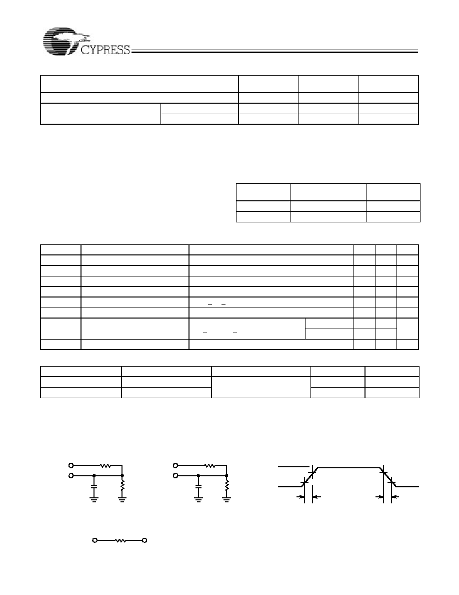
AC Test Loads and Waveforms
C408A≠4
C408A≠5
90%
10%
3.0V
GND
90%
10%
ALL INPUT PULSES
5V
OUTPUT
INCLUDING
JIG AND
SCOPE
5V
OUTPUT
5 pF
INCLUDING
JIG AND
SCOPE
(a)
(b)
5 ns
5 ns
OUTPUT
1.73V
C408A≠6
30 pF
C
L
R1 482
R1 482
R2
256
R2
256
Equivalent to:
TH… VENIN EQUIVALENT
167
CY7C408A
CY7C409A
3
Switching Characteristics
Over the Operating Range
[3, 6]
Test
Conditions
7C408A-15
7C409A-15
7C408A-25
7C409A-25
7C408A-35
7C409A-35
Parameter
Description
Min.
Max.
Min.
Max.
Min.
Max.
Unit
f
O
Operating Frequency
Note 7
15
25
35
MHz
t
PHSI
SI HIGH Time
Note 7
23
11
9
ns
t
PLSI
SI LOW Time
Note 7
25
24
17
ns
t
SSI
Data Set-Up to SI
Note 8
0
0
0
ns
t
HSI
Data Hold from SI
Note 8
30
20
12
ns
t
DLIR
Delay, SI HIGH to IR LOW
35
21
15
ns
t
DHIR
Delay, SI LOW to IR HIGH
40
23
16
ns
t
PHSO
SO HIGH Time
Note 7
23
11
9
ns
t
PLSO
SO LOW Time
Note 7
25
24
17
ns
t
DLOR
Delay, SO HIGH to OR LOW
35
21
15
ns
t
DHOR
Delay, SO LOW to OR HIGH
40
23
16
ns
t
SOR
Data Set-Up to OR HIGH
0
0
0
ns
t
HSO
Data Hold from SO LOW
0
0
0
ns
t
BT
Fall-through, Bubble-back Time
10
65
10
60
10
50
ns
t
SIR
Data Set-Up to IR
Note 9
5
5
5
ns
t
HIR
Data Hold from IR
Note 9
30
20
20
ns
t
PIR
Input Ready Pulse HIGH
Note 10
6
6
6
ns
t
POR
Output Ready Pulse HIGH
Note 11
6
6
6
ns
t
DLZOE
OE LOW to LOW Z (7C408A)
Note 12
35
30
25
ns
t
DHZOE
OE HIGH to HIGH Z (7C408A)
Note 7
35
30
25
ns
t
DHHF
SI LOW to HF HIGH
65
55
45
ns
t
DLHF
SO LOW to HF LOW
65
55
45
ns
t
DLAFE
SO or SI LOW to AFE LOW
65
55
45
ns
t
DHAFE
SO or SI LOW to AFE HIGH
65
55
45
ns
t
PMR
MR Pulse Width
55
45
35
ns
t
DSI
MR HIGH to SI HIGH
25
10
10
ns
t
DOR
MR LOW to OR LOW
55
45
35
ns
t
DIR
MR LOW to IR HIGH
55
45
35
ns
t
LZMR
MR LOW to Output LOW
Note 13
55
45
35
ns
t
AFE
MR LOW to AFE HIGH
55
45
35
ns
t
HF
MR LOW to HF LOW
55
45
35
ns
t
OD
SO LOW to Next Data Out Valid
28
20
16
ns
Notes:
6.
Test conditions assume signal transition time of 5 ns or less, timing reference levels of 1.5V and output loading of the specified I
OL
/I
OH
and 30-pF load
capacitance, as in parts (a) and (b) of AC Test Loads and Waveforms.
7.
1/f
O
> (t
PHSI
+ t
PLSI
), 1/f
O
> (t
PHSO
+ t
PLSO
).
8.
t
SSI
and t
HSI
apply when memory is not full.
9.
t
SIR
and t
HIR
apply when memory is full, SI is high and minimum bubble-through (t
BT
) conditions exist.
10. At any given operating condition t
PIR
> (t
PHSO
required).
11.
At any given operating condition t
POR
> (t
PHSI
required).
12. t
DHZOE
and t
DLZOE
are specified with C
L
= 5 pF as in part (b) of AC Test Loads and Waveforms. t
DHZOE
transition is measured
±
500 mV from steady-state
voltage. t
DLZOE
transition is measured
±
100 mV from steady-state voltage. These parameters are guaranteed and not 100% tested.
13. All data outputs will be at LOW level after reset goes HIGH until data is entered into the FIFO.
CY7C408A
CY7C409A
4
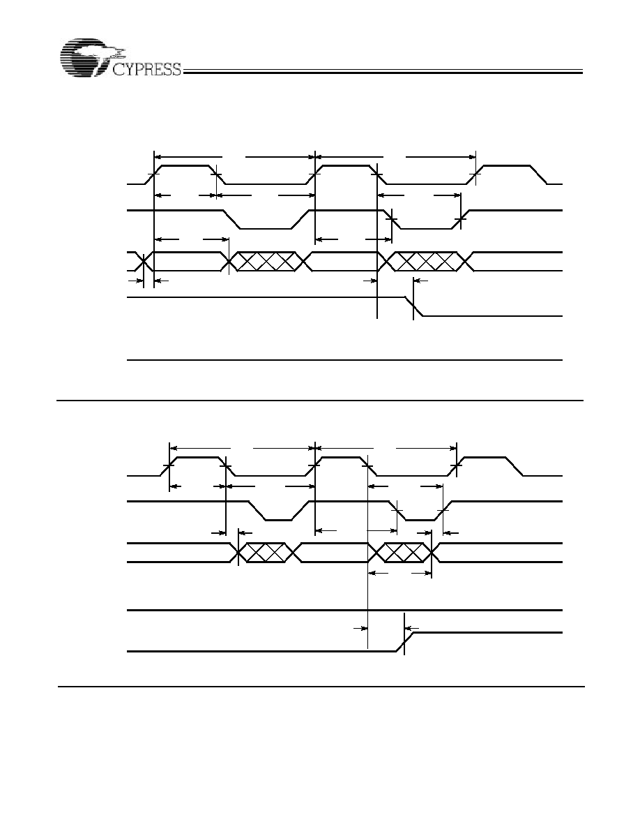
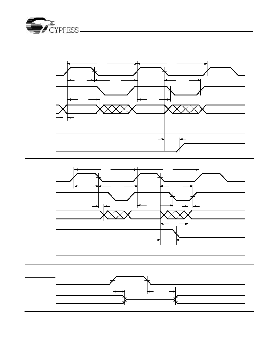
Switching Waveforms
Notes:
14. FIFO contains 8 words.
15. FIFO contains 9 words.
t
DHAFE
Data In Timing Diagram
Data Out Timing Diagram
C408A≠7
C408A≠8
SHIFT IN
I/f
O
I/f
O
t
PHSI
t
PLSI
t
DHIR
t
DLIR
INPUT READY
t
HSI
t
SSI
DATA IN
SHIFT OUT
I/f
O
I/f
O
t
PHSO
t
PLSO
t
DHOR
t
DLOR
OUTPUT READY
t
HSO
DATA OUT
t
SOR
t
DLAFE
AFE
HF
(LOW)
HF
(LOW)
t
OD
AFE
NOTE 14
NOTE 15
CY7C408A
CY7C409A
5
Notes:
16. FIFO contains 31 words.
17. FIFO contains 32 words.
Switching Waveforms
(continued)
t
DLHF
Data In Timing Diagram
Data Out Timing Diagram
C408A≠9
C408A≠10
SHIFT IN
I/f
O
I/f
O
t
PHSI
t
PLSI
t
DHIR
t
DLIR
INPUT READY
t
HSI
t
SSI
DATA IN
SHIFT OUT
I/f
O
I/f
O
t
PHSO
t
PLSO
t
DHOR
t
DLOR
OUTPUT READY
t
HSO
DATA OUT
t
SOR
t
DHHF
AFE
HF
(LOW)
HF
(LOW)
t
OD
AFE
t
DHZOE
Output Enable (CY7C408A only)
C408A≠11
OUTPUT ENABLE
DATA OUT
t
DLZOE
NOTE 16
NOTE 17
NOTE 12