CONFIDENTIAL
PRELIMINARY
enCoReTM II
Low-Speed USB Peripheral Controller
CY7C63310
CY7C638xx
CY7C639xx
Cypress Semiconductor Corporation
·
3901 North First Street
·
San Jose
,
CA 95134
·
408-943-2600
Document 38-08035 Rev. *C
Revised December 13, 2004
1.0
Features
· enCoRe
II USB--"enhanced Component Reduction"
-- Crystalless oscillator with support for an external
crystal or resonator. The internal oscillator
eliminates the need for an external crystal or
resonator
-- Internal 3.3V regulator and internal USB pull-up
resistor
-- Configurable IO for real-world interface without
external components
· USB Specification Compliance
-- Conforms to USB Specification, Version 2.0
-- Conforms to USB HID Specification, Version 1.1
-- Supports one Low-Speed USB device address
-- Supports one control endpoint and two data
endpoints
-- Integrated USB transceiver
· Enhanced 8-bit microcontroller
-- Harvard architecture
-- M8C CPU speed can be up to 24 MHz or sourced by
an external crystal, resonator, or signal
· Internal memory
-- Up to 256 bytes of RAM
-- Up to eight Kbytes of Flash including EEROM
emulation
· Interface can auto-configure to operate as PS/2 or USB
-- No external components for switching between PS/2
and USB modes
-- No GPIO pins needed to manage dual-mode
capability
· Low power consumption
-- Typically 10 mA at 6 MHz
-- 10-uA sleep
· In-system re-programmability
-- Allows easy firmware update
· General-purpose I/O ports
-- Up to 36 General Purpose I/O (GPIO) pins
-- High current drive on GPIO pins. Configurable 8- or
50-mA/pin current sink on designated pins
-- Each GPIO port supports high-impedance inputs,
configurable pull-up, open drain output, CMOS/TTL
inputs, and CMOS output
-- Maskable interrupts on all I/O pins
· 125-mA 3.3V voltage regulator can power external 3.3V
devices
· 3.3V I/O pins
-- 4 I/O pins with 3.3V logic levels
-- Each 3.3V pin supports high-impedance input,
internal pull-up, open drain output or traditional
CMOS output
· SPI serial communication
-- Master or slave operation
-- Configurable up to 2-Mbit/second transfers
-- Supports half duplex single data line mode for
optical sensors
· 2-channel 8-bit or 1-channel 16-bit capture timer.
Capture timers registers store both rising and falling
edge times
-- Two registers each for two input pins
-- Separate registers for rising and falling edge capture
-- Simplifies interface to RF inputs for wireless
applications
· Internal low-power wake-up timer during suspend
mode
-- Periodic wake-up with no external components
· Programmable Interval Timer interrupts
· Reduced RF emissions at 27 MHz and 96 MHz
· Advanced development tools based on Cypress
MicroSystems PSoCTM tools
· Watchdog timer (WDT)
· low-voltage detection with user-configurable threshold
voltages
· Improved output drivers to reduce EMI
· Operating voltage from 4.0V to 5.25VDC
· Operating temperature from 070°C
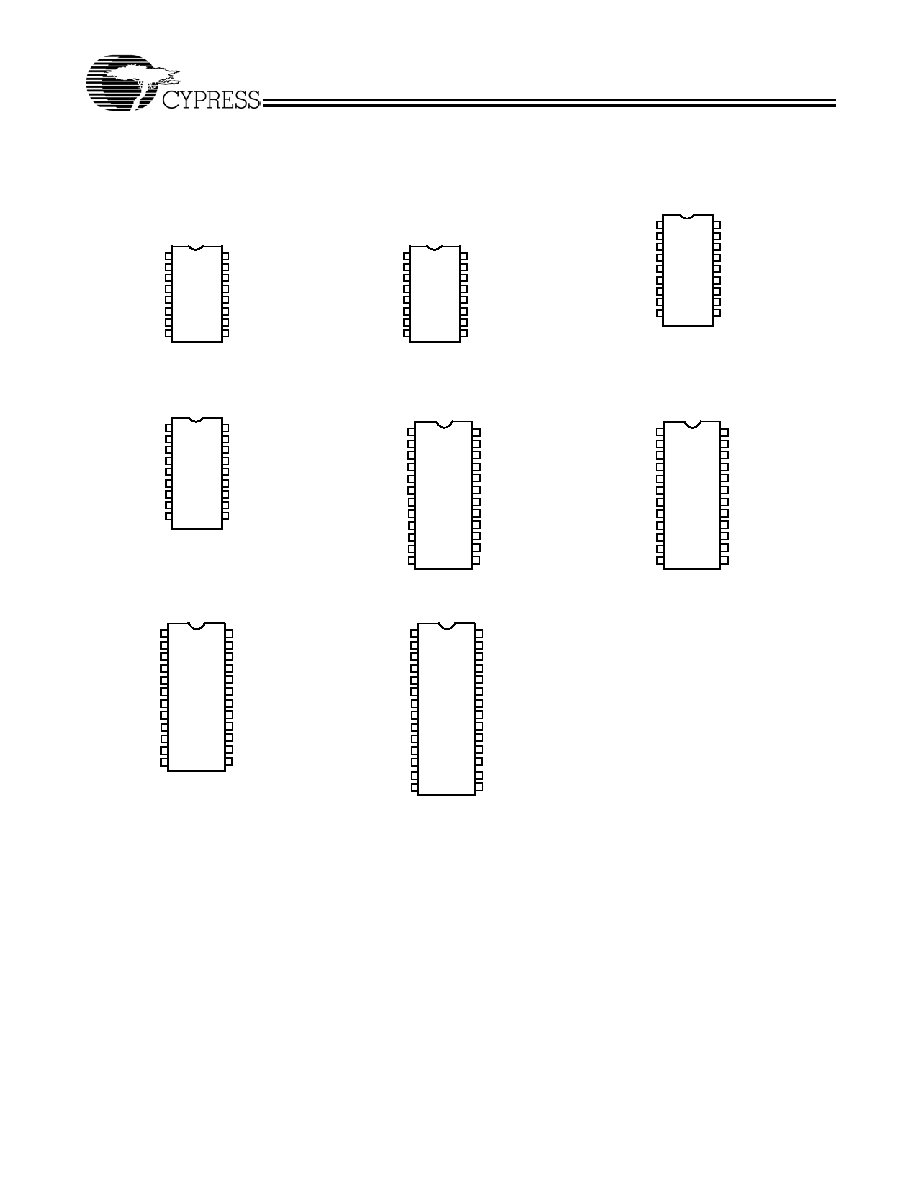
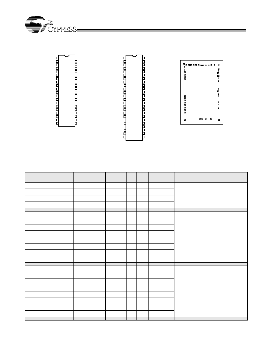
· Available in 16/18/24/40-pin PDIP, 16/18/24-pin SOIC, 24-
pin QSOP, 28/48-pin SSOP, and DIE form
· Industry standard programmer support
1.1
Applications
The CY7C633xx/CY7C638xx/CY7C639xx is targeted for the
following applications:
· PC HID devices
-- Mice (optomechanical, optical, trackball)
-- Keyboards
· Gaming
-- Joysticks
-- Game pads
-- Console keyboards
· General Purpose
-- Barcode scanners
-- POS terminal
-- Consumer electronics
-- Toys
-- Remote controls

CONFIDENTIAL
PRELIMINARY
CY7C63310
CY7C638xx
CY7C639xx
Document 38-08035 Rev. *C
Page 2 of 70
2.0
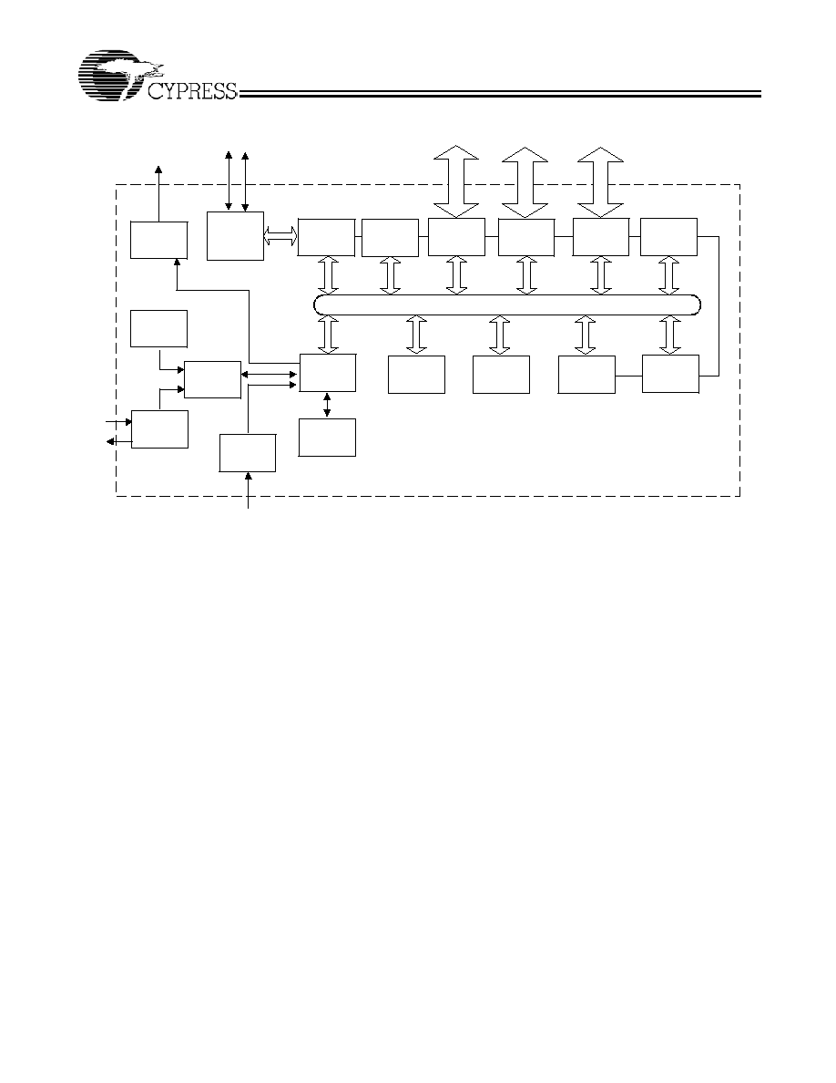
Introduction
Cypress has reinvented its leadership position in the low-
speed USB market with a new family of innovative microcon-
trollers. Introducing enCoRe II USB -- "enhanced Component
Reduction." Cypress has leveraged its design expertise in
USB solutions to advance its family of low-speed USB micro-
controllers, which enable peripheral developers to design new
products with a minimum number of components. The
enCoRe II USB technology builds on to the enCoRe family.
The enCoRe family has an integrated oscillator that eliminates
the external crystal or resonator reducing overall cost. Also
integrated into this chip are other external components
commonly found in low-speed USB applications such as pull-
up resistors, wake-up circuitry, and a 3.3V regulator.
All of this adds up to a lower system cost.
The enCoRe II is 8-bit Flash-programmable microcontroller
with integrated low-speed USB interface. The instruction set
has been optimized specifically for USB and PS/2 operations,
although the microcontrollers can be used for a variety of other
embedded applications.
The enCoRe II features up to 36 general-purpose I/O (GPIO)
pins to support USB, PS/2 and other applications. The I/O pins
are grouped into five ports (Port 0 to 4). The pins on Port 0 and
Port 1 may each be configured individually while the pins on
Ports 2, 3, and 4 may only be configured as a group. Each
GPIO port supports high-impedance inputs, configurable pull-
up, open drain output, CMOS/TTL inputs, and CMOS output
with up to five pins that support programmable drive strength
of up to 50-mA sink current. GPIO Port 1 features four pins that
interface at a voltage level of 3.3 volts. Additionally, each I/O
pin can be used to generate a GPIO interrupt to the microcon-
troller. Each GPIO port has its own GPIO interrupt vector with
the exception of GPIO Port 0. GPIO Port 0 has three dedicated
pins that have independent interrupt vectors (P0.2 - P0.4).
The enCoRe II features an internal oscillator. With the
presence of USB traffic, the internal oscillator can be set to
precisely tune to USB timing requirements (24 MHz ±1.5%).
Optionally, an external 12-MHz or 24-MHz crystal can be used
to provide a higher precision reference for USB operation. The
clock generator provides the 12-MHz and 24-MHz clocks that
remain internal to the microcontroller.
The enCoRe II has up to eight Kbytes of Flash for user's code
and up to 256 bytes of RAM for stack space and user
variables.
In addition, the enCoRe II includes low-voltage reset logic, a
Watchdog timer, a vectored interrupt controller, a 16-bit Free-
Running Timer, and Capture Timers. The low-voltage reset
(LVR) logic detects when power is applied to the device, resets
the logic to a known state, and begins executing instructions
at Flash address 0x0000. The LVR may reset the parts when
Vcc drops below a programmable trip voltage or it may be
configurable to generate a LVR/POR interrupt to inform the
processor about the low-voltage event. The Watchdog timer
can be used to ensure the firmware never gets stalled in an
infinite loop.
The microcontroller supports 23 maskable interrupts in the
vectored interrupt controller. Interrupt sources include a USB
bus reset, LVR/POR, a programmable interval timer, a 1.024-
ms output from the Free Running Timer, three USB endpoints,
two capture timers, five GPIO Ports, three GPIO pins, two SPI,
a 16-bit free running timer wrap, an internal wake-up timer, and
a bus active interrupt. The wake-up timer causes periodic
interrupts when enabled. The USB endpoints interrupt after a
USB transaction complete is on the bus. The capture timers
interrupt whenever a new timer value is saved due to a
selected GPIO edge event. A total of eight GPIO interrupts
support both TTL or CMOS thresholds. For additional flexi-
bility, on the edge sensitive GPIO pins, the interrupt polarity is
programmable to be either rising or falling.
The free-running 16-bit timer provides two interrupt sources:
the programmable interval timer with 1 microsecond resolution
and the 1.024 ms outputs. The timer can be used to measure
the duration of an event under firmware control by reading the
timer at the start and at the end of an event, then calculating
the difference between the two values. The two 8-bit capture
timers save a programmable 8-bit range of the free-running
timer when a GPIO edge occurs on the two capture pins (P0.0,
P0.1). The two 8-bit captures can be ganged into a single 16-
bit capture.
The enCoRe II includes an integrated USB serial interface
engine (SIE) that allows the chip to easily interface to a USB
host. The hardware supports one USB device address with
three endpoints.
The USB D+ and D pins can alternately be used as PS/2
SCLK and SDATA signals so that products can be designed to
respond to either USB or PS/2 modes of operation. PS/2
operation is supported with internal pull-up resistors on SCLK
and SDATA and an interrupt to signal the start of PS/2 activity.
In USB mode the integrated pull-up resistor on D- can be
controlled under firmware. No external components are
necessary for dual USB and PS/2 systems, and no GPIO pins
need to be dedicated to switching between modes. Slow edge
rates operate in both modes to reduce EMI.
The enCoRe II supports in-system programming by using the
D+ and D- pins as the serial programming mode interface. The
programming protocol is not USB.
3.0
Conventions
In this document, bit positions in the registers are shaded to
indicate which members of the enCoRe II family implement the
bits.
Available in all enCoRe II family members
CY7C639xx and CY7C638xx only
CY7C639xx only