2048K x 8 SRAM Module
CYM1481A
Cypress Semiconductor Corporation
∑
3901 North First Street
∑
San Jose
∑
CA 95134
∑
408-943-2600
Document #: 38-05074 Rev. **
Revised September 4, 2001
81A
Features
∑ High-density 16-megabit SRAM modules
∑ High-speed CMOS SRAMs
-- Access time of 70 ns
∑ Low active power
-- 605 mW (max.), 2M x 8
∑ Double-sided SMD technology
∑ TTL-compatible inputs and outputs
∑ Small footprint SIP
-- PCB layout area of 0.72 sq. in.
∑ 2V data retention (L version)
Functional Description
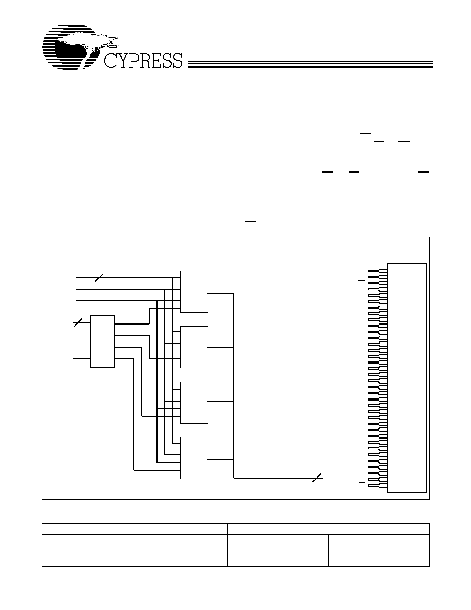
The CYM1481A is a high-performance 16-megabit static RAM
module organized as 2048K words by 8 bits. These modules
are constructed from four 512K x 8 SRAMs in plastic sur-
face-mount packages on an epoxy laminate board with pins.
On-board decoding selects one of the SRAMs from the
high-order address lines, keeping the remaining devices in
standby mode for minimum power consumption.
An active LOW write enable signal (WE) controls the writ-
ing/reading operation of the memory. When MS and WE inputs
are both LOW, data on the eight data input/output pins is writ-
ten into the memory location specified on the address pins.
Reading the device is accomplished by selecting the device
and enabling the outputs MS and OE active LOW while WE
remains inactive or HIGH. Under these conditions, the content
of the location addressed by the information on the address
pins is present on the eight data input/output pins.
The input/output pins remain in a high-impedance state unless
the module is selected, outputs are enabled, and write enable
(WE) is HIGH.
/
Logic Block Diagram
Pin Configuration
1481-1
I/O
0
≠I/O
7
A
0
≠A
18
OE
A
19
≠A
20
WE
MS
SIP
Top View
1 of 4
DECODER
8
2
30
29
28
27
26
25
24
23
22
21
20
19
18
17
16
15
14
13
12
11
10
9
8
7
6
5
4
3
2
1
36
35
34
33
32
31
A
20
I/O
3
I/O
2
WE
V
CC
A
19
I/O
0
A
1
A
2
A
3
A
4
GND
I/O
5
A
10
A
11
A
5
A
13
A
14
MS
A
15
A
16
A
12
A
18
A
6
I/O
1
GND
A
0
A
7
A
8
A
9
I/O
7
I/O
4
I/O
6
A
17
V
CC
OE
512K x 8
SRAM
512K x 8
SRAM
512K x 8
SRAM
512K x 8
SRAM
19
Selection Guide
CYM1481A
Maximum Access Time (ns)
70
85
100
120
Maximum Operating Current (mA)
110
110
110
110
Maximum Standby Current (mA)
64
64
64
64

CYM1481A
Document #: 38-05074 Rev. **
Page 2 of 9
Maximum Ratings
(Above which the useful life may be impaired.)
Storage Temperature ≠55
∞
C to +125
∞
C
Ambient Temperature with
Power Applied0
∞
C to +70
∞
C
Supply Voltage to Ground Potential≠0.3V to +7.0V
DC Voltage Applied to Outputs
in High Z State≠0.3V to +7.0V
DC Input Voltage≠0.3V to +7.0V
Output Current into Outputs (LOW)20 mA
Operating Range
Range
Ambient
Temperature
V
CC
Commercial
0
∞
C to +70
∞
C
5V
±
10%
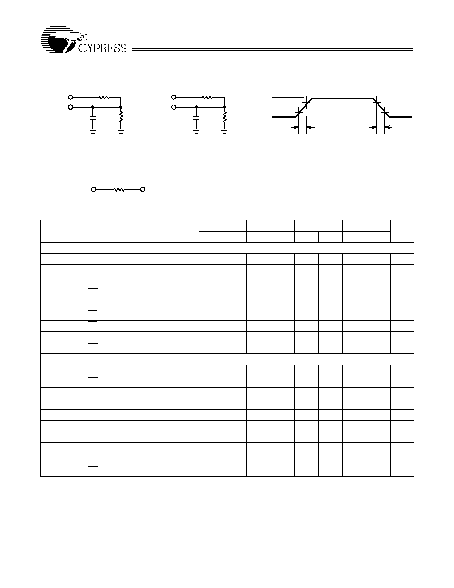
Electrical Characteristics
Over the Operating Range
1481A
Parameter
Description
Test Conditions
Min.
Max.
Unit
V
OH
Output HIGH Voltage
V
CC
= Min., I
OH
= ≠1.0 mA
2.4
V
V
OL
Output LOW Voltage
V
CC
= Min., I
OL
= 2.0 mA
0.4
V
V
IH
Input HIGH Voltage
2.2
V
CC
+ 0.3
V
V
IL
Input LOW Voltage
≠0.3
0.8
V
I
IX
Input Load Current
GND < V
I
< V
CC
≠20
+20
µ
A
I
OZ
Output Leakage Current
GND < V
O
< V
CC
, Output Disabled
≠20
+20
µ
A
I
CC
V
CC
Operating Supply Current V
CC
= Max., MS < V
IL
, I
OUT
= 0 mA
110
mA
I
SB1
Automatic MS
Power-Down Current
Max. V
CC
, MS > V
IH
,
Min. Duty Cycle = 100%
64
mA
I
SB2
Automatic MS
Power-Down Current
Max. V
CC
, MS > V
CC
≠ 0.2V,
V
IN
> V
CC
≠ 0.2V, or V
IN
<
0.2V
Standard
32
mA
L Version
≠100, ≠120
500
µ
A
L Version
≠85
1600
µ
A
Capacitance
[1]
Parameter
Description
Test Conditions
CYM1481AM
ax.
Unit
C
INA
Input Capacitance (A
0≠16
, OE, WE)
T
A
= 25
∞
C, f = 1 MHz,
V
CC
= 5.0V
125
pF
C
INB
Input Capacitance (A
17≠20
, MS)
25
pF
C
OUT
Output Capacitance
165
pF
Note:
1.
Tested on a sample basis.
CYM1481A
Document #: 38-05074 Rev. **
Page 3 of 9
AC Test Loads and Waveforms
1481-3
1481-4
90%
10%
3.0V
GND
90%
10%
ALL INPUT PULSES
5V
OUTPUT
INCLUDING
JIG AND
SCOPE
5V
OUTPUT
5 pF
INCLUDING
JIG AND
SCOPE
(a)
(b)
< 10 ns
< 10 ns
OUTPUT
R1 2530
R2
2830
1340
Equivalent to:
TH… VENIN EQUIVALENT
2.64V
100 pF
R1 2530
R2
2830
1481-2
Switching Characteristics
Over the Operating Range
[2]
1481A-70
1481A≠85
1481A≠100
1481A≠120
Parameter
Description
Min.
Max.
Min.
Max.
Min.
Max.
Min.
Max.
Unit
READ CYCLE
t
RC
Read Cycle Time
70
85
100
120
ns
t
AA
Address to Data Valid
70
85
100
120
ns
t
OHA
Data Hold from Address Change
5
10
10
10
ns
t
AMS
MS LOW to Data Valid
70
85
100
120
ns
t
DOE
OE LOW to Data Valid
40
45
50
60
ns
t
LZOE
OE LOW to Low Z
5
5
5
5
ns
t
HZOE
OE HIGH to High Z
[3]
30
30
35
45
ns
t
LZMS
MS LOW to Low Z
[4]
5
10
10
10
ns
t
HZMS
MS HIGH to High Z
[3, 4]
30
30
35
45
ns
WRITE CYCLE
[5]
t
WC
Write Cycle Time
70
85
100
120
ns
t
SMS
MS LOW to Write End
65
75
90
100
ns
t
AW
Address Set-Up to Write End
65
75
90
100
ns
t
HA
Address Hold from Write End
5
7
7
7
ns
t
SA
Address Set-Up to Write Start
0
5
5
5
ns
t
PWE
WE Pulse Width
65
65
75
85
ns
t
SD
Data Set-Up to Write End
30
35
40
45
ns
t
HD
Data Hold from Write End
0
5
5
5
ns
t
HZWE
WE LOW to High Z
[3]
30
30
35
40
ns
t
LZWE
WE HIGH to Low Z
5
5
5
5
ns
Notes:
2.
Test conditions assume signal transition time of 10
µ
s or less, timing reference levels of 1.5V, input pulse levels of 0 to 3.0V, output loading of 1 TTL load, and
100-pF load capacitance.
3.
t
HZOE
, t
HZMS
, and t
HZWE
are specified with C
L
= 5 pF as in part (b) of AC Test Loads and Waveforms. Transition is measured
±
500 mV from steady-state voltage.
4.
At any given temperature and voltage condition, t
HZMS
is less than t
LZMS
for any given device. These parameters are guaranteed and not 100% tested.
5.
The internal write time of the memory is defined by the overlap of MS LOW and WE LOW. Both signals must be LOW to initiate a write and either signal can
terminate a write by going HIGH. The data input set-up and hold timing should be referenced to the rising edge of the signal that terminates the write.
CYM1481A
Document #: 38-05074 Rev. **
Page 4 of 9
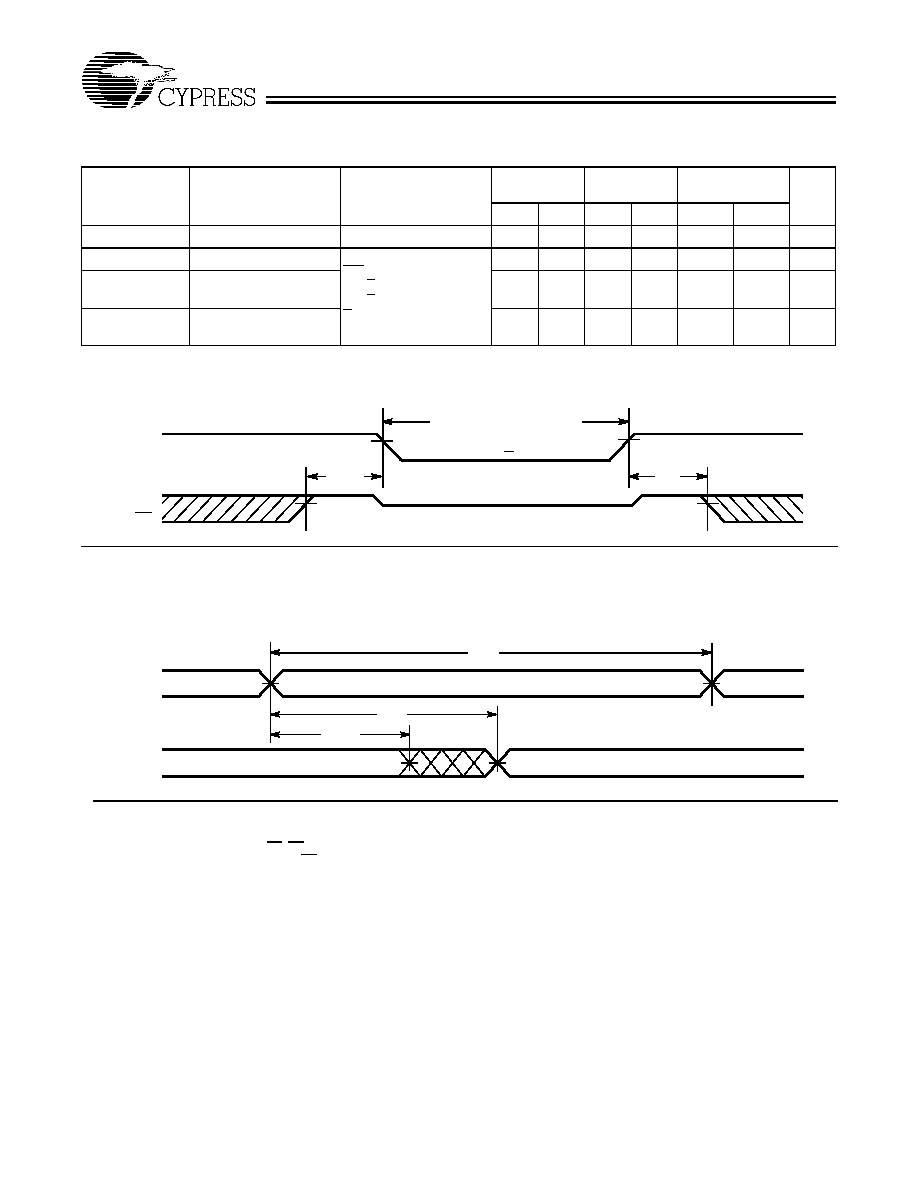
Data Retention Characteristics
(L Version Only)
1481A-70
1481A≠85
1481A≠100
148A1≠120
Parameter
Description
Test Conditions
Min.
Max.
Min.
Max.
Min.
Max.
Unit
V
DR
V
CC
for Retention Data
2
2
2
V
I
CCDR
Data Retention Current
V
DR
= 3.0V,
MS > V
CC
≠ 0.2V,
V
IN
> V
CC
≠ 0.2V or V
IN
< 0.2V
800
800
250
µ
A
t
CDR
[6]
Chip Deselect to Data
Retention Time
0
0
0
ns
t
R
Operation Recovery
Time
5
5
5
ns
Data Retention Waveform
1481-6
4.5V
4.5V
CS
V
CC
t
CDR
V
DR
> 2V
DATA RETENTION MODE
V
DR
t
R
V
IH
V
IH
Switching Waveforms
Notes:
6.
Guaranteed, not tested.
7.
Device is continuously selected. OE, MS = V
IL
.
8.
Address valid prior to or coincident with MS transition LOW.
Read Cycle No. 1
PREVIOUS DATA VALID
DATA VALID
t
RC
t
AA
t
OHA
1481-7
ADDRESS
DATAOUT
[7, 8]
CYM1481A
Document #: 38-05074 Rev. **
Page 5 of 9
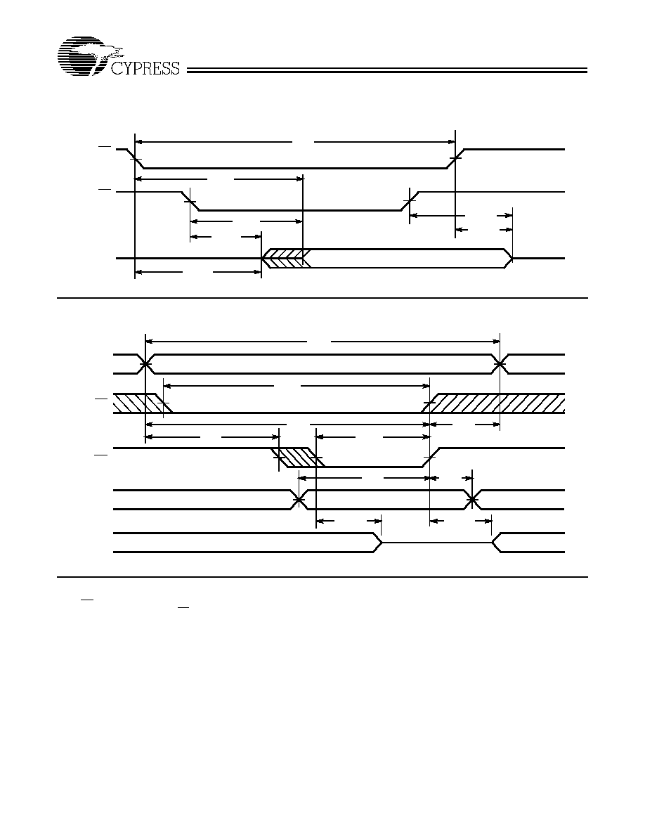
Notes:
9.
WE is HIGH for read cycle.
10. Data I/O is high impedance if OE = V
IH
.
Switching Waveforms (continued)
Read Cycle No. 2
DATA VALID
t
RC
t
AMS
t
DOE
t
LZOE
t
LZMS
HIGH IMPEDANCE
t
HZOE
t
HZMS
HIGH
IMPEDANCE
1481-8
DATA OUT
OE
MS
[8, 9]
Write Cycle No. 1
t
WC
DATA VALID
DATA UNDEFINED
HIGH IMPEDANCE
t
SMS
t
AW
t
SA
t
PWE
t
HA
t
HD
t
HZWE
t
LZWE
t
SD
MS
WE
1481-9
ADDRESS
DATA IN
DATA I/O
[5, 10]