/home/web/doc/html/cypress/171723
Low EMI Spectrum Spread Clock
FS781/82/84
Cypress Semiconductor Corporation
·
3901 North First Street
·
San Jose
·
CA 95134
·
408-943-2600
Document #: 38-07029 Rev. *C
Revised December 14, 2002
Features
· Spread Spectrum clock generator (SSCG) with 1×, 2×,
and 4× outputs
· 6- to 82-MHz operating frequency range
· Modulates external clocks including crystals, crystal
oscillators, or ceramic resonators
· Programmable modulation with simple R-C external
loop filter (LF)
· Center spread modulation
· 3V-5V power supply
· TTL-/CMOS-compatible outputs
· Low short-term jitter
· Low-power Dissipation
-- 3.3 VDC = 37 mW typical
-- 5.0 VDC = 115 mW typical
· Available in 8-pin SOIC and TSSOP packages
Applications
· Desktop/notebook computers
· Printers, copiers, and MFP
· Scanners and fax
· LCD displays and monitors
· CD-ROM, VCD, and DVD
· Automotive and embedded systems
· Networking, LAN/WAN
· Digital cameras and camcorders
· Modems
Benefits
· Programmable EMI reduction
· Fast time to market
· Lower cost of compliance
· No degradation in rise/fall times
· Lower component and PCB layer count
Description
The Cypress FS781/82/84 are Spread Spectrum clock
generator ICs (SSCG) designed for the purpose of reducing
electromagnetic interference (EMI) found in today's
high-speed digital systems.
The FS781/82/84 SSCG clocks use a Cypress-proprietary
technology to modulate the input clock frequency, XIN, by
modulating the frequency of the digital clock. By modulating
the reference clock the measured EMI at the fundamental and
harmonic frequencies of FSOUT is greatly reduced. This
reduction in radiated energy can significantly reduce the cost
of complying with regulatory requirements without degrading
digital waveforms.
The Cypress FS781/82/84 clocks are very simple and
versatile devices to use. By programming the two range select
lines, S0 and S1, any frequency from 6- to 82-MHz operating
range can be selected. The FS781/2/4 are designed to
operate over a very wide range of input frequencies and
provides 1×, 2×, and 4× modulated clock outputs.
The FS78x devices have a simple frequency selection table
that allows operation from 6 MHz to 82 MHz in four separate
ranges. The bandwidth of the frequency spread at FSOUT is
determined by the values of the loop filter components. The
modulation rate is determined internally by the input frequency
and the selected input frequency range.
The Bandwidth of these products can be programmed from as
little as 1.0% up to as much as 4.0% by selecting the proper
loop filter value. Refer to the Loop Filter Selection chart in
Table 2 and Table 3 for the recommended values. Due to a
wide range of application requirements, an external loop filter
(LF) is used on the FS78x products. The user can select the
exact amount of frequency modulation suitable for the appli-
cation. Using a fixed internal loop filter would severely limit
the use of a wide range of modulation bandwidths (Spread %)
to a few discrete values. Refer to FS791/2/4 products for appli-
cations requiring 80- to 140-MHz frequency range.
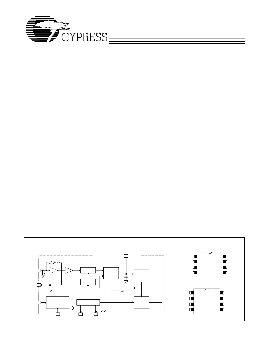
Block Diagram
Pin Configuration
Phase
Detector
VCO
1(3)
2(4)
Xin
Xout
10 pF.
Reference
Divider
8 pF
8 pF
250 K
VCO / N
Modulation
Control
Input Control Logic
Output
Divider
and
Mux
Power Contol
Logic
3(5)
7(1)
8(2)
5(7)
4(6)
VDD
S0
S1
FSOUT
Loop Filter
VSS
6(8)
VSS
VDD
(TSSOP Pin #)
1
2
3
4
8
7
6
5
Xin
Xout
S1
LF
VDD
S0
FSOUT
VSS
FS78x
8 Pin SOIC Package
1
2
3
4
8
7
6
5
S0
VDD
Xin
Xout
FSOUT
VSS
LF
S1
FS78x
8 Pin TSSOP Package
FS781/82/84
Document #: 38-07029 Rev. *C
Page 2 of 11
Output Frequency Selection
Loop Filter Selection Chart
The following table provides a list of recommended loop filter
values for the FS781/82/84. The FS78X is divided into four
ranges and operated at both 3.3V and 5.5 VDC. The loop filter
at the right is representative of the loop filter components in
Table 2.
Pin Description
Pin
Name
I/O
Type
Description
1/2 (SOIC)
3/4 (TSSOP)
X
IN
/X
OUT
I/O
Analog
Pins form an on-chip reference oscillator when connected to terminals
of an external parallel resonant crystal. X
IN
may be connected to
TTL/CMOS external clock source. If X
IN
connected to external clock other
than crystal, leave X
OUT
(pin 2) unconnected.
7/3 (SOIC)
1/5 (TSSOP)
S0 / S1
I
CMOS/TTL
Digital control inputs to select input frequency range and output
frequency scaling. Refer to Table 2 and Table 3 for selection. S0 has internal
pull-down. S1 has internal pull-up.
4 (SOIC)
6 (TSSOP)
LF
I
Analog
Loop Filter. Single ended three-state output of the phase detector. A two-pole
passive loop filter is connected to LF.
6 (SOIC)
8 (TSSOP)
FSOUT
O
CMOS/TTL
Modulated Clock Frequency Output. The center frequency is the same as
the input reference frequency for FS781. Input frequency is multiplied by 2×
and 4× for FS782 and FS784, respectively.
8 (SOIC)
2 (TSSOP)
V
DD
P
Power
Positive Power Supply.
5 (SOIC)
7 (TSSOP)
V
SS
P
Power
Power Supply Ground.
Table 1. FSOUT SSCG (Modulated Output Clock) Product Selection
Product Number
FSOUT Frequency Scaling
Description
FS781
1×
1× modulated frequency of input clock
FS782
2×
2× modulated frequency of input clock
FS784
4×
4× modulated frequency of input clock
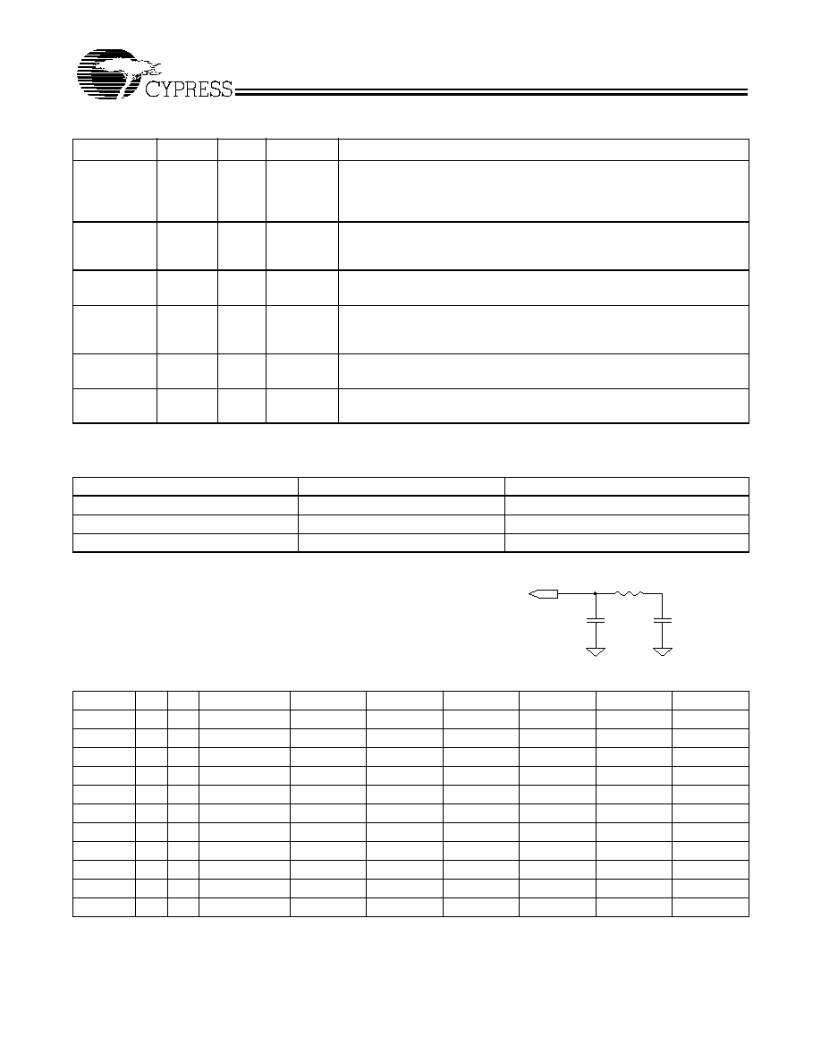
C8
R6
C7
LF (pin 4)
Table 2. FS781/82/84 Recommended Loop Filter Values C7 (pF) @ +3.3 VDC ±5% (R6 = 3.3K)
[1, 2, 3, 4]
Input MHz
S1
S0
BW = 1.0%
[3]
BW = 1.5%
[3]
BW = 2.0%
[3]
BW = 2.5%
[3]
BW = 3.0%
[3]
BW = 3.5%
[3]
BW = 4.0%
[3]
6
0
0
10,000/1000
1550
910
780
700
640
560
8
0
0
10,000/330
990
820
640
520
450
400
10
0
0
1040
680
460
360
300
240
210
12
0
0
830
420
300
220
200
190
170
14
0
0
580
230
200
160
140
100
80
16
0
1
10000
980
760
580
470
410
385
18
0
1
1200
750
580
470
415
370
300
20
0
1
1000
730
470
390
320
220
190
22
0
1
960
640
410
270
230
200
180
24
0
1
920
400
250
210
180
160
150
26
0
1
660
300
220
180
150
140
120
Notes:
1.
If the value selected from the above chart is not a standard, use the next available larger value.
2.
All bandwidths indicated above are total peak-to-peak spread. 1% = +0.5% to 0.5%. 4% = +2.0% to 2.0%.
3.
If C8 is not listed in the chart for a particular bandwidth and frequency, it is not used in the loop filter.
4.
Contact Cypress for LF values less than 1.0% bandwidth.
FS781/82/84
Document #: 38-07029 Rev. *C
Page 3 of 11
28
0
1
470
230
180
150
130
100
70
30
0
1
470
180
140
120
100
80
60
32
0
1
330
170
120
100
82
68
47
34
1
0
10000
860
640
520
430
380
330
36
1
0
2200
820
620
470
400
330
290
38
1
0
1500
690
520
410
340
290
240
40
1
0
960
600
420
340
280
220
160
42
1
0
940
620
380
275
230
210
180
44
1
0
950
680
400
250
210
190
170
46
1
0
900
580
270
220
190
180
165
48
1
0
790
440
260
210
180
160
140
50
1
0
660
360
250
190
170
150
140
52
1
0
470
325
220
185
155
135
120
54
1
0
470
270
200
170
140
130
100
56
1
0
445
250
185
150
120
85
47
58
1
0
430
210
165
130
100
65
33
60
1
0
295
185
150
120
100
90
82
62
1
0
270
220
150
120
100
82
68
64
1
1
1180
860
560
410
340
290
230
65
1
1
1180
850
540
400
330
280
220
66
1
1
1180
760
560
350
260
220
210
68
1
1
1180
750
500
320
260
230
210
70
1
1
1120
740
470
370
300
240
170
72
1
1
1160
780
470
300
250
220
190
74
1
1
1110
770
470
280
230
210
190
76
1
1
1000
720
440
240
210
190
170
78
1
1
910
670
270
210
190
170
160
80
1
1
900
620
260
210
190
170
156
82
1
1
900
540
250
210
190
170
150
Table 2. FS781/82/84 Recommended Loop Filter Values C7 (pF) @ +3.3 VDC ±5% (R6 = 3.3K)
[1, 2, 3, 4]
(continued)
Input MHz
S1
S0
BW = 1.0%
[3]
BW = 1.5%
[3]
BW = 2.0%
[3]
BW = 2.5%
[3]
BW = 3.0%
[3]
BW = 3.5%
[3]
BW = 4.0%
[3]
Table 3. FS781/82/84 Recommended Loop Filter Values C7 (pF) @ +5.0 VDC ±5% (R6 = 3.3K)
[1, 2, 3, 4]
Input MHz
S1
S0
BW = 1.0%
[3]
BW = 1.5%
[3]
BW = 2.0%
[3]
BW = 2.5%
[3]
BW = 3.0%
[3]
BW = 3.5%
[3]
BW = 4.0%
[3]
6
0
0
1140
1030
930
830
710
610
510
8
0
0
1170
970
740
570
460
400
280
10
0
0
1030
660
430
350
280
210
130
12
0
0
760
340
230
200
180
160
130
14
0
0
450
240
180
140
100
70
50
16
0
1
2490
970
730
590
480
430
370
18
0
1
2490
870
650
510
430
370
310
20
0
1
1360
680
480
370
280
190
250
22
0
1
990
560
330
260
230
200
190
24
0
1
820
360
250
200
180
160
150
26
0
1
530
270
210
170
150
110
90
28
0
1
430
230
180
150
110
100
90
FS781/82/84
Document #: 38-07029 Rev. *C
Page 4 of 11
30
0
1
250
200
150
110
100
90
80
32
1
0
Note 4
1000
740
570
470
410
370
34
1
0
Note 4
990
710
520
420
360
300
36
1
0
Note 4
970
670
480
380
310
230
38
1
0
Note 4
880
560
380
310
270
220
40
1
0
Note 4
800
460
290
240
230
220
42
1
0
1030
680
360
260
220
200
190
44
1
0
790
560
260
220
200
190
170
46
1
0
1110
420
280
210
180
170
140
48
1
0
1110
280
200
190
170
140
120
50
1
0
830
330
200
180
160
130
110
52
1
0
560
340
205
170
140
120
90
54
1
0
510
280
180
140
110
110
90
56
1
0
470
210
160
120
100
90
90
58
1
0
450
220
250
110
90
80
80
60
1
0
430
240
120
90
80
80
70
62
1
1
Note 4
800
580
430
330
250
180
64
1
1
Note 4
720
490
375
285
200
140
66
1
1
Note 4
630
400
320
240
150
100
68
1
1
Note 4
690
365
285
225
170
140
70
1
1
Note 4
650
330
250
210
190
180
72
1
1
Note 4
575
340
250
210
190
170
74
1
1
Note 4
500
355
245
205
180
165
76
1
1
Note 4
550
330
230
200
175
160
78
1
1
Note 4
600
290
220
190
170
155
80
1
1
Note 4
570
240
210
185
165
150
82
1
1
Note 4
540
250
200
180
160
140
Table 3. FS781/82/84 Recommended Loop Filter Values C7 (pF) @ +5.0 VDC ±5% (R6 = 3.3K)
[1, 2, 3, 4]
(continued)
Input MHz
S1
S0
BW = 1.0%
[3]
BW = 1.5%
[3]
BW = 2.0%
[3]
BW = 2.5%
[3]
BW = 3.0%
[3]
BW = 3.5%
[3]
BW = 4.0%
[3]
FS781/82/84
Document #: 38-07029 Rev. *C
Page 5 of 11
SSCG Modulation Profile
The digital control inputs S0 and S1 determine the modulation
frequency of FS781/2/4 products. The input frequency is
divided by a fixed number, depending on the operating range
that is selected. The modulation frequency of the FS78x can
be determined from Table 4. To compute the modulation
frequency, determine the values of S0 and S1, and find the
modulation divider number in Table 4.
Theory of Operation
The FS781/82/84 devices are phase-lock loop-(PLL)-type
clock generators using Direct Digital Synthesis (DDS). `By
precisely controlling the bandwidth of the output clock, the
FS781/2/4 products become a low-EMI clock generator. The
theory and detailed operation of these products will be
discussed in the following sections.
EMI
All clocks generate unwanted energy in their harmonics.
Conventional digital clocks are square waves with a duty cycle
that is very close to 50%. Because of the 50/50 duty cycle,
digital clocks generate most of their harmonic energy in the
odd harmonics (e.g., third, fifth, seventh). It is possible to
reduce the amount of energy contained in the fundamental
and harmonics by increasing the bandwidth of the funda-
mental clock frequency. Conventional digital clocks have a
very high Q factor, which means that all of the energy at that
frequency is concentrated in a very narrow bandwidth, conse-
quently, higher energy peaks. Regulatory agencies test
electronic equipment by the amount of peak energy radiated
from the equipment. By reducing the peak energy at the funda-
mental and harmonic frequencies, the equipment under test is
able to satisfy agency requirements for EMI. Conventional
methods of reducing EMI have been to use shielding, filtering,
multi-layer PCBs, etc. These FS781/2 and 4 reduce the peak
energy in the clock by increasing the clock bandwidth and
lowering the Q of the clock.
SSCG
The FS781/82/84 products use a unique method of modulating
the clock over a very narrow bandwidth and controlled rate of
change, both peak to peak and cycle to cycle. The FS78x
products take a narrow band digital reference clock in the
range of 6 82 MHz and produce a clock that sweeps between
a controlled start and stop frequency and precise rate of
change. To understand what happens to an SSCG clock,
consider that we have a 20-MHz clock with a 50% duty cycle.
From a 20-MHz clock we know the following:
Clock Frequency = Fc = 20 MHz.
Clock Period = Tc = 1/20 MHz = 50 ns.
Consider that this 20-MHz clock is applied to the X
IN
input of
the FS78x as either an externally driven clock or the result of
a parallel resonant crystal connected to pins 1 and 2 of the
FS78x. Also consider that the products are operating from a
5V DC power supply and the loop filter is set for a total
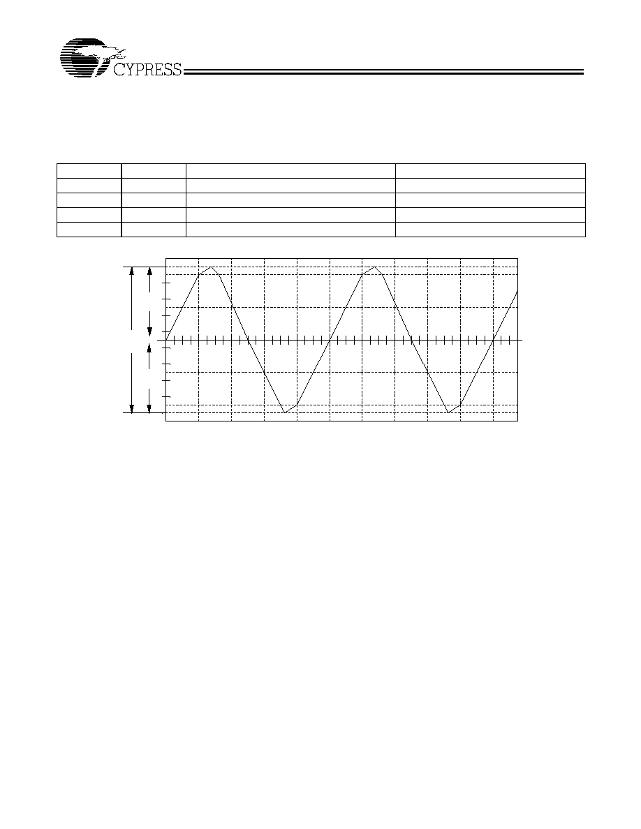
bandwidth spread of 2%. Refer to
Figure 2.
Table 4. Modulation Rate Divider Ratios
S1
S0
Input Frequency Range (MHz)
Modulation Divider Number
0
0
6 to 16
120
0
1
16 to 32
240
1
0
32 to 66
480
1
1
66 to 82
720
Note:
5.
With the correct loop filter connected to Pin 4, the following profile will provide the best EMI reduction. This profile can be seen on a Time Domain Analyzer.
Xin
+ .5%
- .5%
TIME (microseconds)
1.0%
Total
Figure 1. Frequency Profile in Time Domain
[5]