 | –≠–ª–µ–∫—Ç—Ä–æ–Ω–Ω—ã–π –∫–æ–º–ø–æ–Ω–µ–Ω—Ç: FS786/87 | –°–∫–∞—á–∞—Ç—å:  PDF PDF  ZIP ZIP |

Low EMI Spread Spectrum Clock
Cypress Semiconductor Corporation
Document#: 38-07031 Rev. *A
12/14/02
http://www.cypress
Page 1 of 13
APPROVED PRODUCT
FS786/787
Features
∑
Spread Spectrum Clock Generator (SSCG)
with 1x Spread and 1X non-Spread Output.
∑
6 to 82 MHz operating frequency range.
∑
Modulates external clocks including crystals,
crystal oscillators and ceramic resonators.
∑
Programmable modulation with simple
R-C external loop filter (LF)
∑
Provides Two Output Clocks, One Modulated
and One Non-Modulated clock.
∑
Center Spread Modulation.
∑
3 - 5 Volt power supply.
∑
TTL/CMOS compatible outputs.
∑
Low short term jitter.
∑
Low Power Dissipation;
3.3 VDC = 37 mW ≠ typical
5.0 VDC = 115 mW - typical
∑
Available in 8 pin SOIC package.
Applications
∑
Desktop/Notebook
Computers
∑
Printers, Copiers and MFP
∑
Scanners and Fax
∑
LCD Displays and Monitors
∑
CD-ROM, VCD and DVD
∑
Automotive and Embedded Systems
∑
Networking,
LAN/WAN
∑
Digital Cameras and Camcorders
∑
Modems
Benefits
∑
Programmable EMI Reduction
∑
Fast Time to Market
∑
Lower cost of compliance
∑
No degradation in Rise/Fall times
∑
Lower component and PCB layer count
Product Description
The CYPRESS FS786/787 are Spread Spectrum
Clock Generator ICs (SSCG) designed for the
purpose of reducing Electro Magnetic Interference
(EMI) found in today's high-speed digital systems.
The FS786/787 SSCG clocks use an Cypress
proprietary technology to modulate the input clock
frequency, FSOUT
by modulating the frequency of
the digital clock. By modulating the reference clock
the measured EMI at the fundamental and harmonic
frequencies of FSOUT is greatly reduced. This
reduction in radiated energy can significantly reduce
the cost of complying with regulatory requirements
without degrading digital waveforms.
The CYPRESS FS786/787 clocks are very simple
and versatile devices to use. Range selection is
performed via one pin, D0. The FS786/787 are
designed to operate over a very wide range of input
frequencies and provide one modulated and one
non-modulated output.
The FS786/787 devices have a simple frequency
selection table that allows operation from 6 MHz to
82 MHz in two separate ranges and two separate
parts. The bandwidth of the frequency spread at
FSOUT is determined by the values of the loop filter
components. The modulation rate is determined
internally by the input frequency and the selected
input frequency range.
The Bandwidth of these products can be
programmed from as little as 0.6% up to as much as
4.0% by selecting the proper loop filter value. Refer
to the Loop Filter Selection chart on page 6 for
recommended values. Due to a wide range of
application requirements, an external loop filter (LF)
is used on the FS786/787 products. The user can
select the exact amount of frequency modulation
suitable for the application. Using a fixed internal
loop filter would severely limit the use of a wide
range of modulation bandwidths (Spread %) to a few
discrete values.
Refer to FS791/2/4 products for applications
requiring 80 to 140 MHz frequency range.
Low EMI Spread Spectrum Clock
Cypress Semiconductor Corporation
Document#: 38-07031 Rev. *A
12/14/02
http://www.cypress
Page 2 of 13
APPROVED PRODUCT
FS786/787
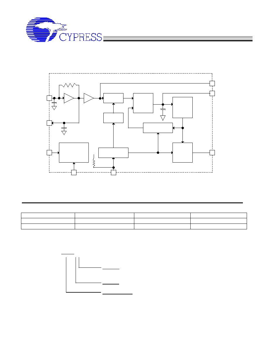
Block Diagram
Figure 1.
Ordering Information
Product Number
Frequency Range
Package Type
Production Flow
FS786BZ
16 ≠ 32 MHz, 64 ≠ 82 MHz
8 Pin 150 mil SOIC
Commercial, 0 to 70
∞
C
FS787BZ
6 ≠ 14 MHz, 34 ≠ 62 MHz
8 Pin 150 mil SOIC
Commercial, 0 to 70
∞
C
Marking Example:
Date Code
FS786BZB (FS787BZB)
Lot Number
FS786BZ
Package
Z = SOIC (150 Mil)
Revision
Device Number
Phase
Detector
VCO
1
2
Xin
Xout
10 pF.
Reference
Divider
8 pF
8 pF
250 K
VCO / N
Modulation
Control
Input Control Logic
Output
Divider
and
Mux
Power Contol
Logic
3
8
5
4
VDD
D0
FSOUT
Loop Filter
VSS
7
VDD
6
REFOUT
Low EMI Spread Spectrum Clock
Cypress Semiconductor Corporation
Document#: 38-07031 Rev. *A
12/14/02
http://www.cypress
Page 3 of 13
APPROVED PRODUCT
FS786/787
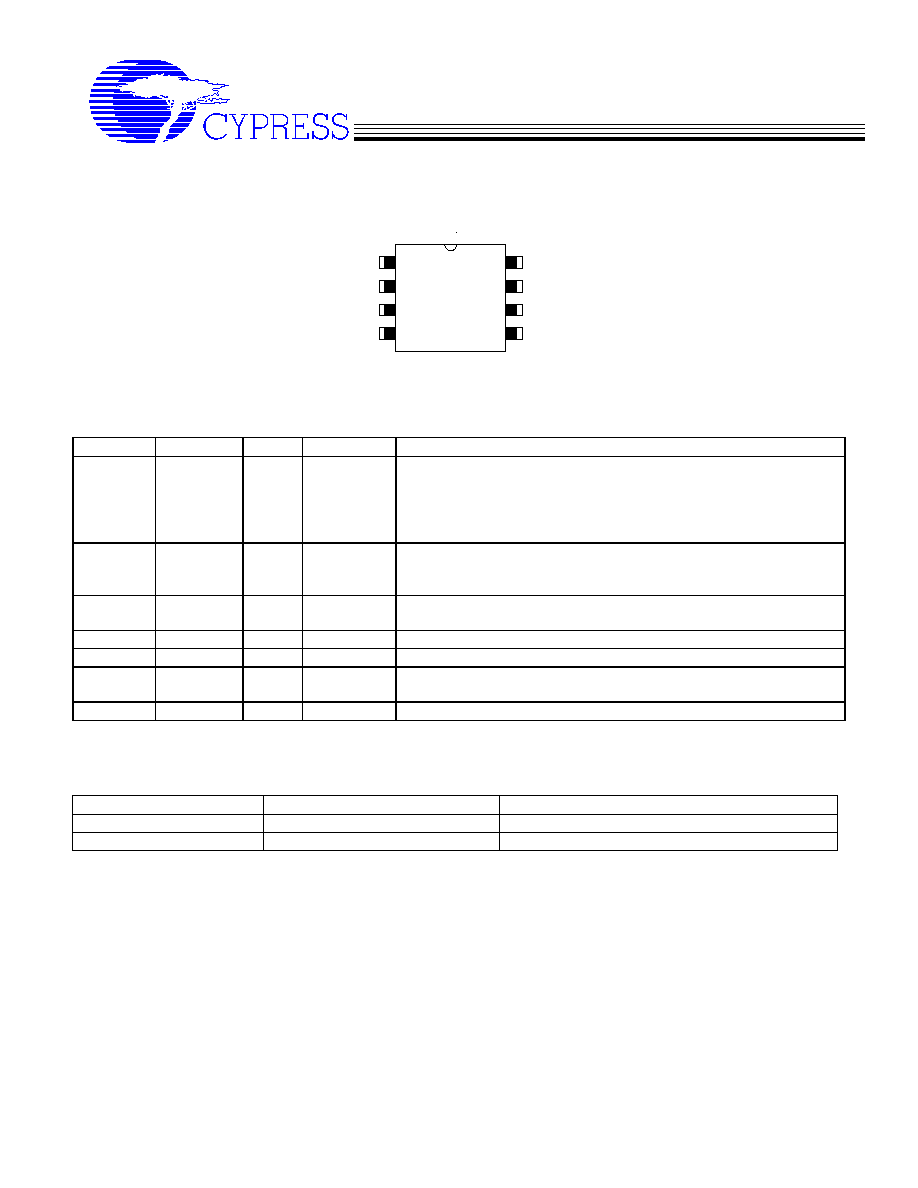
Pin Configuration
Refer to page 11 for package dimensions.
Pin Description
Pin No.
Pin Name
I/O
TYPE
Description
1/2
Xin / Xout
I/O
Analog
Pins form an on-chip reference oscillator when connected to
terminals of an external parallel resonant crystal. Xin may be
connected to TTL/CMOS external clock source. If Xin
connected to external clock other than crystal, leave Xout (pin 2)
unconnected.
3
D0
I
CMOS/TTL
Input frequency range selection. Has internal pull-up resistor.
FS786
≈
0 = 16 ≠ 32 MHz, 1 = 64 ≠ 82 MHz.
FS787
≈
0 = 6 ≠ 14 MHz, 1 = 34 ≠ 62 MHz.
4
LF
I
Analog
Loop Filter. Single ended tri-state output of the phase detector. A
passive RC filter is connected to the Loop Filter pin (LF).
5
VSS
P
Power
Power Supply Ground.
6
REFOUT
O
CMOS/TTL
Non-Modulated Clock Output of Reference Oscillator.
7
FSOUT
O
CMOS/TTL
Modulated Clock Output of Reference Oscillator. Frequency is
center spread and 1X of reference clock.
8
VDD
P
Power
Positive Power Supply.
Table 1. Pin Description
Output Frequency Selection
Product Number
FSOUT Frequency Scaling
Description
FS786
1x
1X Modulated Clock + 1X Non-Modulated Clock
FS787
1x
1X Modulated Clock + 1X Non-Modulated Clock
Table 2. FSOUT SSCG (Modulated Output Clock) Product Selection
1
2
3
4
8
7
6
5
Xin
Xout
LF
VDD
FSOUT
VSS
FS786/787
D0
REFOUT
Low EMI Spread Spectrum Clock
Cypress Semiconductor Corporation
Document#: 38-07031 Rev. *A
12/14/02
http://www.cypress
Page 4 of 13
APPROVED PRODUCT
FS786/787
This device contains circuitry to protect the inputs against damage due to high static voltages or electric fields;
however, precautions should be taken to avoid application of any voltage higher than the absolute maximum rated
voltages to this circuit. For proper operation, Vin and Vout should be constrained to the range, VSS < ( Vin or
Vout) < VDD. All digital inputs are tied high or low internally. Refers to electrical specifications for operating
supply range.
Absolute Maximum Ratings
1
Item
Symbol
Min
Max
Units
Operating Voltage
VDD
3.0
6.0
VDC
Input, relative to VSS
VIRvss
-0.3
VDD +0.3
VDC
Output, relative to VSS
VORvss
-0.3
VDD +0.3
VDC
AVDD relative to DVDD
Vpp
-100
+100
mV
AVSS relative to DVSS
Vss
-100
+100
mV
Temperature, Operating
TOP
0
+ 70
0
C
Temperature, Storage
TST
- 65
+ 150
0
C
Table 3
Electrical Characteristics
Characteristic
Symbol
Min
Typ
Max
Units
Input Low Voltage
VIL
-
-
0.3 * VDD
VDC
Input High Voltage
VIH
0.7 * VDD
-
-
VDC
Input Low Current
IIL
-
-
100
µ
A
Input High Current
IIH
-
-
100
µ
A
Output Low Voltage IOL= 10mA, VDD = 5V
VOL
-
-
0.4
VDC
Output High Voltage IOH = 10mA, VDD = 5V
VOH
VDD-1.0
-
-
VDC
Output Low Voltage IOL= 6mA, VDD = 3.3V
VOL
-
-
0.4
VDC
Output High Voltage IOH = 5mA,VDD = 3.3V
VOH
2.4
-
-
VDC
Resistor, Pull Up (Pin-3)
Rpu
60K
125K
200K
Ohms
Input Capacitance (Pin-1)
C
in1
-
8
-
pF
Output Capacitance (Pin-2)
C
in2
-
8
-
pF
5 Volt Dynamic Supply Current (C
L =
No Load)
ICC
-
38
-
mA
3.3 Volt Dynamic Supply Current (C
L =
No Load)
ICC
-
20
-
mA
Short Circuit Current (FSOUT)
ISC
-
25
-
mA
Test measurements performed at VDD = 3.3V and 5.0V
±
10%, Xin = 48 MHz, Ta = 0
∞
C to 70
∞
C
Table 4
1
Single Power Supply: The Voltage on any input or I/O pin cannot exceed the power pin during power-up.

Low EMI Spread Spectrum Clock
Cypress Semiconductor Corporation
Document#: 38-07031 Rev. *A
12/14/02
http://www.cypress
Page 5 of 13
APPROVED PRODUCT
FS786/787
Timing Characteristics
Characteristic
Symbol
Min.
Typ.
Max.
Units
FSOUT Rise Time @ 10 - 90% at 5 VDC
tTLH
2.0
2.2
2.5
ns
FSOUT Fall Time @ 10 - 90% at 5 VDC
tTHL
1.7
2.0
2.2
ns
FSOUT Rise Time @ 0.8 - 2.0V at 5 VDC
tTLH
0.50
0.65
0.75
ns
FSOUT Fall Time @ 0.8 - 2.0V at 5 VDC
tTHL
0.50
0.65
0.75
ns
FSOUT Rise Time @ 10 - 90% at 3.3 VDC
tTLH
2.6
2.65
2.9
ns
FSOUT Fall Time @ 10 - 90% at 3.3 VDC
tTHL
2.0
2.1
2.2
ns
FSOUT Rise Time @ 0.8 - 2.0V at 3.3 VDC
tTLH
0.8
0.95
1.1
ns
FSOUT Fall Time @ 0.8 - 2.0V at 3.3 VDC
tTHL
0.78
0.85
0.9
ns
FSOUT Duty Cycle @ 50% of VDD
TsymF1
45
50
55
%
FSOUT, Cycle to Cycle Jitter, 48 MHz @ 3.30 VDC
CCJ
-
320
370
ps
FSOUT, Cycle to Cycle Jitter, 48 MHz @ 5.00 VDC
CCJ
-
310
360
ps
FSOUT, Cycle to Cycle Jitter, 72 MHz @ 3.30 VDC
CCJ
-
270
325
ps
FSOUT, Cycle to Cycle Jitter, 72 MHz @ 5.00 VDC
CCJ
-
390
440
ps
REFOUT Rise Time @ 10 ≠ 90% at 5 VDC
tTLH
4.2
4.5
4.9
ns
REFOUT Fall Time @ 10 ≠ 90% at 5 VDC
tTHL
2.5
2.65
2.8
ns
REFOUT Rise Time @ 0.8 ≠ 2.0 V at 5 VDC
tTLH
0.74
0.80
0.86
ns
REFOUT Fall Time @ 0.8 ≠ 2.0 V at 5 VDC
tTHL
0.76
0.85
0.93
ns
REFOUT Rise Time @ 10 ≠ 90% at 3.3 VDC
tTLH
4.6
4.95
5.3
ns
REFOUT Fall Time @ 10 ≠ 90% at 3.3 VDC
tTHL
2.5
2.65
2.8
ns
REFOUT Rise Time @ 0.8 ≠ 2.0 V at 3.3 VDC
tTLH
1.4
1.5
1.6
ns
REFOUT Fall Time @ 0.8 ≠ 2.0 V at 3.3 VDC
tTHL
1.00
1.1
1.2
ns
Unless otherwise indicated, measurements performed at VDD = 3.3 and 5.0V
±
10%, Ta = 0
∞
C to 70
∞
C, CL = 15pF, Xin
= 48 MHz.
Table 5
Application Selection Table
Select the row containing the frequency for the intended application. Read the device number and D0
programming in cells to the right of Fin. The Modulation Rate is also given below.
Fin (MHz)
(pin 1/2)
D0
(pin 3)
Modulation
Rate
Device to Use
6 ≠ 14
0
Fin/120
FS787BZB
16 ≠ 32
0
Fin/240
FS786BZB
34 - 62
1
Fin/480
FS787BZB
64 - 82
1
Fin/720
FS786BZB
Table 6