
Low EMI Spectrum Spread Clock
FS791/92/94
Cypress Semiconductor Corporation
∑
3901 North First Street
∑
San Jose
∑
CA 95134
∑
408-943-2600
Document #: 38-07343 Rev *A
Revised December 28, 2002
92/94
Features
∑ Spread Spectrum Clock Generator (SSCG) with 1x, 2x
and 4x outputs
∑ 80- to 140-MHz operating frequency range
∑ Modulates external clocks including crystals, crystal
oscillators, and ceramic resonators
∑ Programmable modulation with simple R-C external
loop filter (LF)
∑ Center spread modulation
∑ 3≠5 Volt power supply
∑ TTL/CMOS compatible outputs
∑ Low short-term jitter
∑ Low Power Dissipation;
-- 3.3 VDC = 73 mW--typical
-- 5.0 VDC = 225 mW--typical
∑ Available in 8-pin SOIC package
.
Applications
∑ Desktop/Notebook computers
∑ VGA, XGA, and SXGA LCD displays
∑ High-speed printers and copiers
∑ CD-ROM, VCD, and DVD
∑ Embedded systems
∑ Networking, LAN/WAN
∑ Modems
Benefits
∑ Programmable EMI reduction
∑ Fast time-to-market
∑ Lower cost of compliance
∑ No degradation in Rise/Fall time
∑ Lower component and PCB layer count
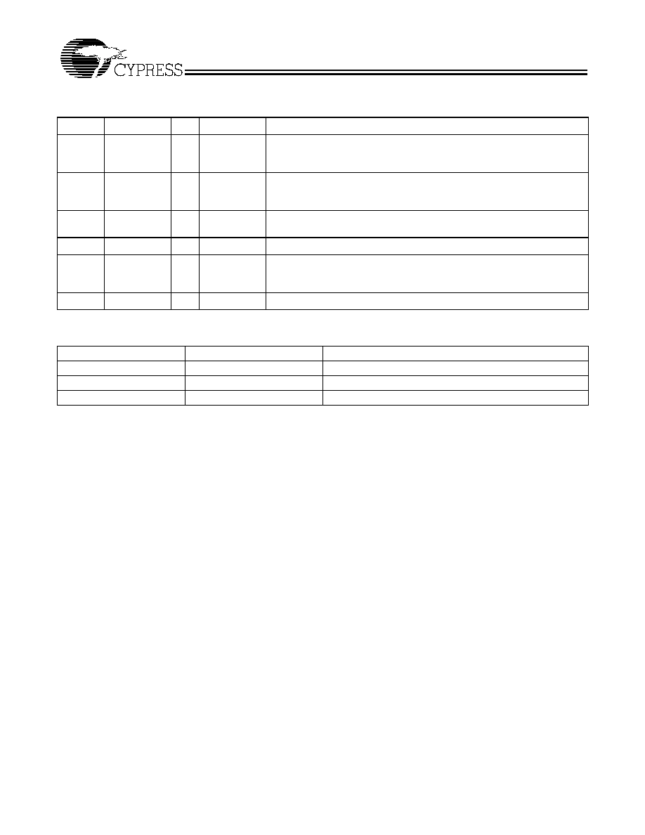
Block Diagram
Pin Configuration
Phase
Detector
VCO
1
2
Xin
Xout
10 pF.
Reference
Divider
10 pF.
10 pF.
VCO / N
Modulation
Control
Input Control
Counter
and
Mux
Power Contol
Logic
3
7
8
5
4
VDD
S0
S1
FSOUT
Loop Filter
VSS
6
1
2
3
4
8
7
6
5
Xin
Xout
S1
LF
VDD
S0
FSOUT
VSS
FS79x
FS791/92/94
Document #: 38-07343 Rev *A
Page 2 of 9
.
General Description
The Cypress FS791/2/4 are Spread Spectrum Clock Genera-
tor ICs (SSCG) designed for the purpose of reducing Electro
Magnetic Interference (EMI) found in today's high-speed digi-
tal systems.
The FS791/2/4 SSCG clocks use an Cypress proprietary tech-
nology to modulate the input clock frequency, FSOUT,
by mod-
ulating the frequency of the digital clock. By modulating the
reference clock the measured EMI at the fundamental and har-
monic frequencies of FSOUT is greatly reduced. This reduc-
tion in radiated energy can significantly reduce the cost of
complying with regulatory requirements without degrading dig-
ital waveforms.
The FS791/2/4 are designed to operate over a very wide range
of input frequencies and provide 1x, 2x, and 4x modulated
clock outputs.
The bandwidth of the frequency spread at FSOUT is deter-
mined by the values of the loop filter components. The modu-
lation rate is determined internally by the input frequency and
the selected input frequency range.
The bandwidth of these products can be programmed from as
little as 0.6% up to as much as 4.0% by selecting the proper
loop filter value. Refer to the Loop Filter Selection chart on
page 4 for recommended values. Due to a wide range of ap-
plication requirements, an external loop filter (LF) is used on
the FS79x products.
The user can select the exact amount of frequency modulation
suitable for the application. Using a fixed internal loop filter
would severely limit the use of a wide range of modulation
bandwidths (Spread%) to a few discrete values.
The Cypress FS791/2/4 Spread Spectrum Clock Generator
(SSCG) products are versatile devices to use in a wide range
of applications.
Refer to FS781/2/4 products for applications requiring a 6 to
82 MHz frequency range.
Pin Description
Pin
Name
I/O
Type
Description
1,2
Xin/Xout
I/O
analog
Pins form an on-chip reference oscillator when connected to terminals of an
external parallel resonant crystal. XIN may be connected to TTL/CMOS ex-
ternal clock other than crystal, leave XOUT (pin 2) unconnected.
3,7
S1/S0
I
CMOS/TTL
Digital control inputs used to select the input frequency range and output
frequency scaling. Refer Table 1 for selection.
S1 has internal pull-up(1) and S0 has internal pull-down(0).
4
LF
I
Analog
Loop filter. Single ended three-state output of the phase detector. A sin-
gle-pole low-pass filter is connected to the loop filter (LF).
5
VSS
P
Power
Power Supply Ground.
6
FSOUT
O
CMOS/TTL
Modulated Clock Output. The output frequency is centered on and a multiple
of the input (Xin) as follows:
FS791 = 1X; FS792 = 2X; FS794 = 4X
8
VDD
P
Power
Positive Power Supply.
Table 1. Output Frequency Selection ≠ FSOUT SSCG (Modulated Output Clock) Product Selection
Product Number
FSOUT Frequency Scaling
Description
FS791
1X
1X Modulated Frequency of Input Clock
FS792
2X
2X Modulated Frequency of Input Clock
FS794
4X
4X Modulated Frequency of Input Clock

FS791/92/94
Document #: 38-07343 Rev *A
Page 3 of 9
Absolute Maximum Ratings
[1, 2]
Parameter
Description
Min.
Max.
Unit
V
DD
Operating Voltage
3.0
6.0
VDC
VIR
VSS
Input, relative to V
SS
≠0.3
V
DD
+ 0.3
VDC
VOR
VSS
Output, relative to V
SS
≠0.3
V
DD
+ 0.3
VDC
V
PP
AV
DD
relative to DV
DD
≠100
+100
mV
V
SS
AV
SS
relative to DV
SS
≠100
+100
mV
T
OP
Temperature, operating
0
+70
∞C
T
ST
Temperature, Storage
≠65
+150
∞C
Table 2. DC Electrical Characteristics: Test measurements performed at V
DD
= 3.3V and 5.0V ±10%, Xin = 100 MHz, Ta =
0∞C to 70∞C
Parameter
Description
Min.
Typ.
Max.
Unit.
V
IL
Input Low Voltage
0.8
VDC
V
IH
Input High Voltage
2.0
VDC
I
IL
Input Low Current
100
µ
A
I
IH
Input High Current
100
µ
A
V
OL
Output Low Voltage I
OL
= 10 mA, V
DD
= 5V
0.4
VDC
V
OH
Output High Voltage I
OH
= 10 mA, V
DD
= 5V
V
DD
≠ 1.0
VDC
V
OL
Output Low Voltage I
OL
= 6 mA, V
DD
= 3.3V
0.4
VDC
V
OH
Output High Voltage I
OH
= 5 mA, V
DD
= 3.3V
2.4
VDC
C
in1
Input Capacitance (Pin-1)
6
8
10
pF
C
in2
Output Capacitance (Pin-2)
6
8
10
pF
I
CC
5-Volt Dynamic Supply Current (C
L =
O)
45
55
mA
I
CC
3.3-Volt Dynamic Supply Current (C
L =
O)
22
28
mA
I
SC
Short Circuit Current (FM-OUT)
25
VDC
Table 3. Timing Characteristics: Test measurements performed at V
DD
= 3.3V and 5.0V ±10%, Ta = 0∞C to 70∞C, CL = 20 pF,
Xin = 100 MHz
Parameter
Description
Min.
Typ.
Max.
Unit
t
TLH
Output Rise Time Measured at 10% - 90% @ 5 VDC
2.0
2.2
2.5
ns
t
THL
Output Fall Time Measured at 10% - 90% @ 5 VDC
1.7
2.0
2.2
ns
t
TLH
Output Rise Time Measured at 0.8V - 2.0V @ 5 VDC
0.50
0.65
0.75
ns
t
THL
Output Fall Time Measured at 0.8V - 2.0 V @ 5 VDC
0.50
0.65
0.75
ns
t
TLH
Output Rise Time Measured at 10% - 90% @ 3.3 VDC
2.60
2.65
2.90
ns
t
THL
Output Fall Time Measured at 10% - 90% @ 3.3 VDC
2.00
2.10
2.20
ns
t
TLH
Output Rise Time Measured at 0.8V - 2.0V @ 3.3 VDC
0.80
0.95
1.10
ns
t
THL
Output Fall Time Measured at 0.8V - 2.0 V @ 3.3 VDC
0.78
0.85
0.90
ns
T
symF1
Output Duty Cycle
45
50
55
%
t
j1s
Peak-to Peak Jitter One Sigma
-
150
250
ps
Note:
1.
Single Power Supply: The voltage on any input or I/O pin cannot excceed the power pin during power-up.
2.
This device contains circuitry to protect the inputs against damage due to high static voltages or electric fields; however, precautions should be taken to avoid
application of any voltage higher than the absolute maximum rated voltages to this circuit. For proper operation, V
in
and V
out
should be constrained to the
range, V
SS
< (V
in
or V
out
) < V
DD
. All digital inputs are tied HIGH or LOW internally. Refers to electrical specifications for operating supply range.
FS791/92/94
Document #: 38-07343 Rev *A
Page 4 of 9
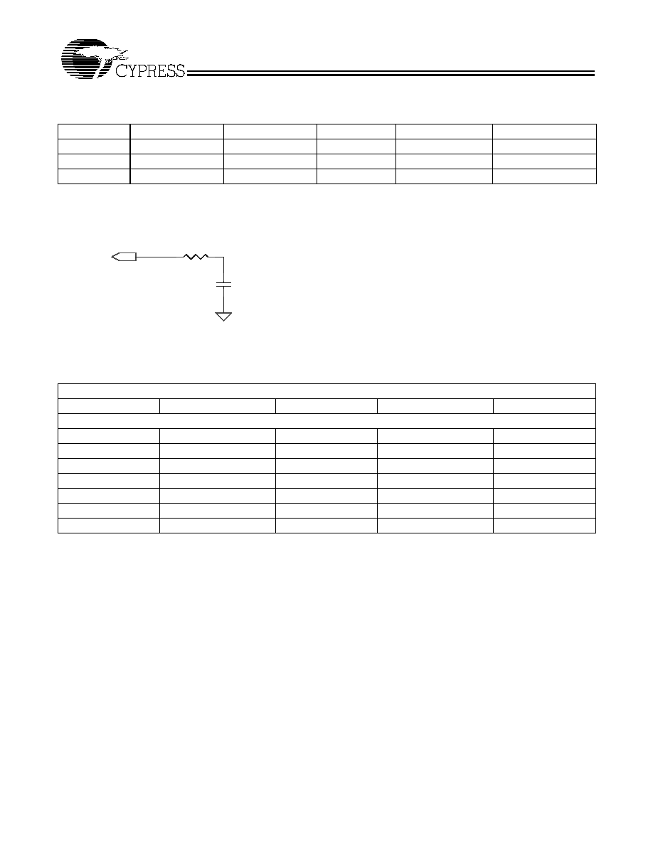
Loop Filter Selection Chart
Table 5 provides a list of recommended loop filter values for
the FS791/2/4. The FS79x products operate at both 3.3 and
5.0VDC. The loop filter shown in Figure 1 is representative of
the loop filter components in Table 5
SSCG Modulation Profile
The modulation frequency of the FS79x can be computed di-
viding the input frequency by this 720. The formula to compute
the Modulation Frequency is Fm = fin / 720.
Example: Fin
= 108 MHz
Range =
1,1
Fm
= 108 MHz / 720 = 150 kHz
With the correct loop filter connected to pin 4, the following
profile will provide the best EMI reduction. This profile can be
seen on a Time Domain Analyzer. See Figure 3.
Table 4. Range Selection Table
[3]
Part Number
S1 (Pin 3)
S0 (Pin 7)
Fin (Pin 1 & 2)
Modulation Rate
FSOUT (Pin 6)
FS791
1
1
80≠140MHz
Fin/720
80≠140MHz
FS792
1
0
40≠70MHz
Fin/480
80≠140MHz
FS794
0
1
20≠35MHz
Fin/240
80≠140MHz
R6
C7
LF (pin 4)
Figure 1. Loop Filter Selection
Table 5. FS79x Recommended Loop Filter Values
[4]
+3.3 to 5.0VDC, ±5% (R6 = 3.3K)
Input (MHz)
BW = 1% (note 5)
BW = 2% (note 5)
BW = 3% (note 5)
BW = 4% (note 5)
All C7 capacitor values are in picofarads (pF)
80
1000
220
190
170
90
510
190
130
90
100
250
150
96
65
110
200
120
74
47
120
150
80
52
38
130
120
55
33
26
140
100
43
22
16
Notes:
3.
Fin is the frequency of the crystal connected to pins 1 & 2 to form an oscillator circuit or the frequency of a clock source connected to pin 1, derived from other
means. When the clock source is from other than a crystal, pin 2 must be left unconnected.
4.
Component values are industry standards and are readily available from component suppliers.
5.
All bandwidths indicated above are total peak-to-peak spread, example: 1% = +0.5% to ≠0.5% and 4% = +2.0% to ≠2.0%

FS791/92/94
Document #: 38-07343 Rev *A
Page 5 of 9
SSCG Theory of Operation
The FS791/2/4 devices are Phase-Locked Loop (PLL) type
clock generators using Direct Digital Synthesis (DDS). By pre-
cisely controlling the bandwidth of the output clock, the
FS791/792/794 products become Low EMI clock generators.
The theory and detailed operation of these products will be
discussed in the following sections.
EMI
All clocks generate unwanted energy in their harmonics. Con-
ventional digital clocks are square waves with a duty cycle that
is very close to 50%. Because of the 50/50 duty cycle, digital
clocks generate most of their harmonic energy in the odd har-
monics, i.e.; 3
rd
, 5
th
, 7
th
etc. It is possible to reduce the amount
of energy contained in the fundamental and harmonics by in-
creasing the bandwidth of the fundamental clock frequency.
Conventional digital clocks have a very high Q factor, which
means that all of the energy at that frequency is concentrated
in a very narrow bandwidth, consequently, higher energy
peaks. Regulatory agencies test electronic equipment by the
amount of peak energy radiated from the equipment. By re-
ducing the peak energy at the fundamental and harmonic fre-
quencies, the equipment under test is able to satisfy agency
requirements for Electro-Magnetic Interference (EMI). Con-
ventional methods of reducing EMI have been to use shield-
ing, filtering, multi-layer PCBs etc. The FS791/2/4 products
use the approach of reducing the peak energy in the clock by
increasing the clock bandwidth, and lowering the Q of the
clock.
SSCG
The FS791/2/4 products use a unique method of modulating
the clock over a very narrow bandwidth and controlled rate of
change, both peak-to-peak and cycle-to-cycle. The FS79x
products take a narrow band digital reference clock in the
range 80≠140 MHz and produce a clock that sweeps between
a controlled start and stop frequency and precise rate of
change. To understand what happens to an SSCG clock, con-
sider that we have a 100-MHz clock with a 50% duty cycle.
From a 100-MHz clock we know the following;
Clock Frequency = fc = 100 MHz
Clock Period = Tc =1/100 MHz = 10 ns
Consider that this 100-MHz clock is applied to the Xin input of
the FS79x, either as an externally driven clock or as the result
of a parallel resonant crystal connected to pins 1 and 2 of the
FS79x. Also consider that the products are operating from a
5-volt DC power supply and the loop filter is set for a total
bandwidth spread of 2%. Refer to Table 5 on page 4.
From the above parameters, the output clock at FSOUT will
be sweeping symmetrically around a center frequency of
100 MHz.
The minimum and maximum extremes of this clock will be
+1.0 MHz and ≠1.0 MHz. So, we have a clock that is sweeping
from 99.0 MHz to 101.0 MHz and back again. If we were to
look at this clock on a spectrum analyzer we would see the
picture in Figure 4. Keep in mind that this is a drawing of a
perfect clock with no noise.
Xin
+ .5%
- .5%
TIME (microseconds)
1.0%
Total
Figure 2. Frequency Profile in Time Domain
50%
50%
Figure 3. Unmodulated Clock