256K x 36/512K x 18 Pipelined SRAM
CY7C1366A/GVT71256C36
CY7C1367A/GVT71512C18
Cypress Semiconductor Corporation
∑
3901 North First Street
∑
San Jose
∑
CA 95134
∑
408-943-2600
June 12, 2001
Features
∑ Fast access times: 2.5 ns, 3.0 ns, and 3.5 ns
∑ Fast clock speed: 225 MHz, 200 MHz, 166 MHz, and
150 MHz
∑ Fast OE access times: 2.5 ns, 3.0 ns, and 3.5 ns
∑ Optimal for performance (two cycle chip deselect, depth
expansion without wait state)
∑ 3.3V ≠5% and +10% power supply
∑ 3.3V or 2.5V I/O supply
∑ 5V tolerant inputs except I/Os
∑ Clamp diodes to V
SS
at all inputs and outputs
∑ Common data inputs and data outputs
∑ Byte Write Enable and Global Write control
∑ Multiple chip enables for depth expansion:
three chip enables for TA(GVTI)/A(CY) package version
and two chip enables for B(GVTI)/BG(CY) and
T(GVTI)/AJ(CY) package versions
∑ Address pipeline capability
∑ Address, data and control registers
∑ Internally self-timed Write Cycle
∑ Burst control pins (interleaved or linear burst
sequence)
∑ Automatic power-down for portable applications
∑ JTAG boundary scan for B and T package version
∑ Low profile 119-bump, 14-mm x 22-mm PBGA (Ball Grid
Array) and 100-pin TQFP packages
Functional Description
The Cypress Synchronous Burst SRAM family employs
high-speed, low power CMOS designs using advanced
triple-layer polysilicon, double-layer metal technology. Each
memory cell consists of four transistors and two high valued
resistors.
The CY7C1366A/GVT71256C36 and CY7C1367A/
GVT71512C18 SRAMs integrate 262,144 x 36 and 524,288 x
18 SRAM cells with advanced synchronous peripheral circuitry
and a 2-bit counter for internal burst operation. All synchro-
nous inputs are gated by registers controlled by a
positive-edge-triggered Clock Input (CLK). The synchronous
inputs include all addresses, all data inputs, address-pipelin-
ing Chip Enable (CE), depth-expansion Chip Enables (CE
2
and CE
2
), Burst Control Inputs (ADSC, ADSP, and ADV), Write
Enables (BWa, BWb, BWc, BWd, and BWE), and Global Write
(GW). However, the CE
2
Chip Enable input is only available for
the TA(GVTI)/A(CY) package version.
Asynchronous inputs include the Output Enable (OE) and
Burst Mode Control (MODE). The data outputs (Q), enabled
by OE, are also asynchronous.
Addresses and chip enables are registered with either Ad-
dress Status Processor (ADSP) or Address Status Controller
(ADSC) input pins. Subsequent burst addresses can be inter-
nally generated as controlled by the Burst Advance Pin (ADV).
Address, data inputs, and write controls are registered on-chip
to initiate a self-timed WRITE cycle. WRITE cycles can be one
to four bytes wide, as controlled by the write control inputs.
Individual byte write allows an individual byte to be written.
BWa controls DQa. BWb controls DQb. BWc controls DQc.
BWd controls DQd. BWa, BWb, BWc, and BWd can be active
only with BWE being LOW. GW being LOW causes all bytes
to be written. The x18 version only has 18 data inputs/outputs
(DQa and DQb) along with BWa and BWb (no BWc, BWd,
DQc, and DQd).
For the B(GVTI)/BG(CY) and T(GVTI)/AJ(CY) package ver-
sions, four pins are used to implement JTAG test capabilities:
Test Mode Select (TMS), Test Data-In (TDI), Test Clock (TCK),
and Test Data-Out (TDO). The JTAG circuitry is used to serially
shift data to and from the device. JTAG inputs use
LVTTL/LVCMOS levels to shift data during this testing mode of
operation. The TA package version does not offer the JTAG
capability.
The CY7C1366A/GVT71256C36 and CY7C1367A/
GVT71512C18 operate from a +3.3V power supply. All inputs
and outputs are LVTTL compatible.
Selection Guide
7C1366A-225/
71256C36-4.4
7C1367A-225/
71512C18-4.4
7C1366A-200/
71256C36-5
7C1367A-200/
71512C18-5
7C1366A-166/
71256C36-6
7C1367A-166/
71512C18-6
7C1366A-150/
71256C36-6.7
7C1367A-150/
71512C18-6.7
Maximum Access Time (ns)
2.5
3.0
3.5
3.5
Maximum Operating Current (mA)
Commercial
570
510
425
380
Maximum CMOS Standby Current (mA)
10
10
10
10
CY7C1366A/GVT71256C36
CY7C1367A/GVT71512C18
3
Pin Configurations
A
A
A
A
A1
A0
TM
S
TD
I
V
SS
V
CC
TD
O
TC
K
A
A
A
A
A
A
A
DQb
DQb
DQb
V
CCQ
V
SS
DQb
DQb
DQb
DQb
V
SS
V
CCQ
DQb
DQb
V
SS
NC
V
CC
ZZ
DQa
DQa
V
CCQ
V
SS
DQa
DQa
DQa
DQa
V
SS
V
CCQ
DQa
DQa
DQa
DQc
DQc
DQc
V
CCQ
V
SS
DQc
DQc
DQc
DQc
V
SS
V
CCQ
DQc
DQc
V
CC
NC
V
SS
DQd
DQd
V
CCQ
V
SS
DQd
DQd
DQd
DQd
V
SS
V
CCQ
DQd
DQd
DQd
A
A
CE
CE
2
BW
d
BW
c
BW
b
BW
a
A
V
CC
V
SS
CL
K
GW
BW
E
OE
AD
S
C
AD
S
P
AD
V
A
A
1
2
3
4
5
6
7
8
9
10
11
12
13
14
15
16
17
18
19
20
21
22
23
24
25
26
27
28
29
30
31
32
33
34
35
36
37
38
39
40
41
42
43
44
45
46
47
48
49
50
80
79
78
77
76
75
74
73
72
71
70
69
68
67
66
65
64
63
62
61
60
59
58
57
56
55
54
53
52
51
10
0
99
98
97
96
95
94
93
92
91
90
89
88
87
86
85
84
83
82
81
MO
D
E
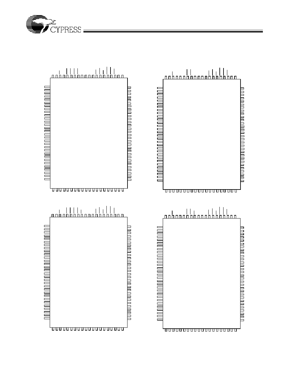
CY7C1366A/GVT71256C36
(256K X 36)
NC
A
NC
NC
V
CCQ
V
SS
NC
DPa
DQa
DQa
V
SS
V
CCQ
DQa
DQa
V
SS
NC
V
CC
ZZ
DQa
DQa
V
CCQ
V
SS
DQa
DQa
NC
NC
V
SS
V
DDQ
NC
NC
NC
NC
NC
NC
V
CCQ
V
SS
NC
NC
DQb
DQb
V
SS
V
CCQ
DQb
DQb
V
CC
NC
V
SS
DQb
DQb
V
CCQ
V
SS
DQb
DQb
DQb
NC
V
SS
V
CCQ
NC
NC
NC
A
A
CE
CE
2
NC
NC
BW
b
BW
a
A
V
CC
V
SS
CLK
GW
BW
E
OE
AD
SC
AD
SP
AD
V
A
A
1
2
3
4
5
6
7
8
9
10
11
12
13
14
15
16
17
18
19
20
21
22
23
24
25
26
27
28
29
30
31
32
33
34
35
36
37
38
39
40
41
42
43
44
45
46
47
48
49
50
80
79
78
77
76
75
74
73
72
71
70
69
68
67
66
65
64
63
62
61
60
59
58
57
56
55
54
53
52
51
10
0
99
98
97
96
95
94
93
92
91
90
89
88
87
86
85
84
83
82
81
CY7C1367A/GVT71512C18
(512K x 18)
NC
100-Pin TQFP
Top View
A
A
A
A
A1
A0
NC
NC
V
SS
V
CC
NC
A
A
A
A
A
A
A
A
DQb
DQb
DQb
V
CCQ
V
SS
DQb
DQb
DQb
DQb
V
SS
V
CCQ
DQb
DQb
V
SS
NC
V
CC
ZZ
DQa
DQa
V
CCQ
V
SS
DQa
DQa
DQa
DQa
V
SS
V
CCQ
DQa
DQa
DQa
DQc
DQc
DQc
V
CCQ
V
SS
DQc
DQc
DQc
DQc
V
SS
V
CCQ
DQc
DQc
V
CC
NC
V
SS
DQd
DQd
V
CCQ
V
SS
DQd
DQd
DQd
DQd
V
SS
V
CCQ
DQd
DQd
DQd
A
A
CE
CE
2
BW
d
BW
c
BW
b
BW
a
CE
2
V
CC
V
SS
CL
K
GW
BW
E
OE
AD
SC
AD
SP
AD
V
A
A
1
2
3
4
5
6
7
8
9
10
11
12
13
14
15
16
17
18
19
20
21
22
23
24
25
26
27
28
29
30
31
32
33
34
35
36
37
38
39
40
41
42
43
44
45
46
47
48
49
50
80
79
78
77
76
75
74
73
72
71
70
69
68
67
66
65
64
63
62
61
60
59
58
57
56
55
54
53
52
51
10
0
99
98
97
96
95
94
93
92
91
90
89
88
87
86
85
84
83
82
81
MO
D
E
CY7C1366A/GVT71256C36
(256K X 36)
NC
A
NC
NC
V
CCQ
V
SS
NC
DPa
DQa
DQa
V
SS
V
CCQ
DQa
DQa
V
SS
NC
V
CC
ZZ
DQa
DQa
V
CCQ
V
SS
DQa
DQa
NC
NC
V
SS
V
CCQ
NC
NC
NC
NC
NC
NC
V
CCQ
V
SS
NC
NC
DQb
DQb
V
SS
V
CCQ
DQb
DQb
V
CC
NC
V
SS
DQb
DQb
V
CCQ
V
SS
DQb
DQb
DQb
NC
V
SS
V
CCQ
NC
NC
NC
A
A
CE
CE
2
NC
NC
BW
b
BW
a
CE
2
V
CC
V
SS
CLK
GW
BW
E
OE
AD
SC
AD
SP
AD
V
A
A
1
2
3
4
5
6
7
8
9
10
11
12
13
14
15
16
17
18
19
20
21
22
23
24
25
26
27
28
29
30
31
32
33
34
35
36
37
38
39
40
41
42
43
44
45
46
47
48
49
50
80
79
78
77
76
75
74
73
72
71
70
69
68
67
66
65
64
63
62
61
60
59
58
57
56
55
54
53
52
51
10
0
99
98
97
96
95
94
93
92
91
90
89
88
87
86
85
84
83
82
81
CY7C1367A/GVT71512C18
(512K x 18)
NC
TA Package Version
TA Package Version
T Package Version
T Package Version
A
A
A
A
A1
A0
TM
S
TD
I
V
SS
V
CC
TD
O
TC
K
A
A
A
A
A
A
A
MO
D
E
A
A
A
A
A1
A0
NC
NC
V
SS
V
CC
NC
A
A
A
A
A
A
A
A
MO
D
E
CY7C1366A/GVT71256C36
CY7C1367A/GVT71512C18
5
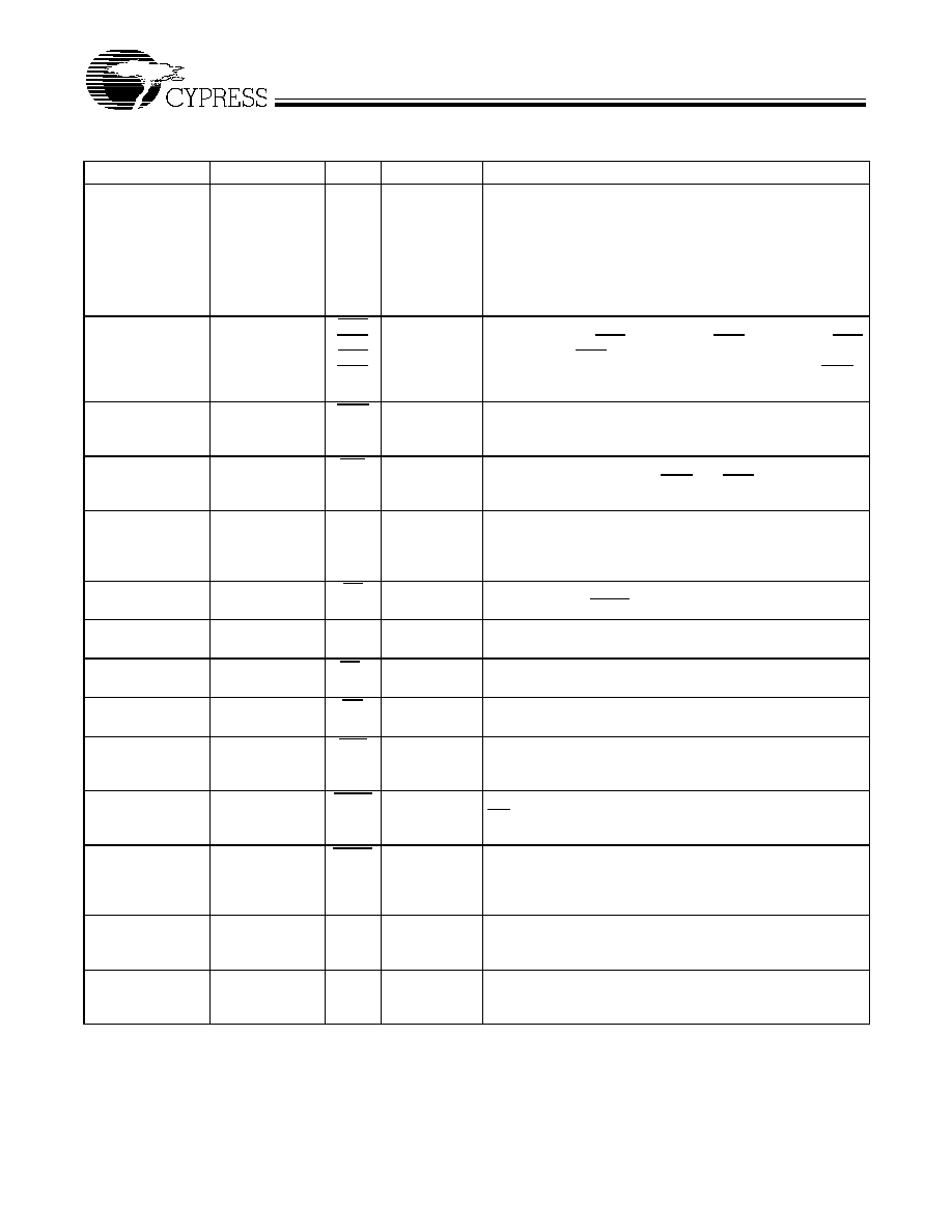
256K X 36 Pin Descriptions
X36 PBGA Pins
X36 QFP Pins
Name
Type
Description
4P
4N
2A, 3A, 5A, 6A, 3B,
5B, 6B, 2C, 3C, 5C,
6C, 2R, 6R, 3T, 4T,
5T
37
36
35, 34, 33, 32,
100, 99, 82, 81,
44, 45, 46, 47,
48, 49, 50
92 (T Version)
43 (TA Version)
A0
A1
A
Input-
Synchronous
Addresses: These inputs are registered and must meet the set
up and hold times around the rising edge of CLK. The burst
counter generates internal addresses associated with A0 and
A1, during burst cycle and wait cycle.
5L
5G
3G
3L
93
94
95
96
BWa
BWb
BWc
BWd
Input-
Synchronous
Byte Write: A byte write is LOW for a WRITE cycle and HIGH
for a READ cycle. BWa controls DQa. BWb controls DQb. BWc
controls DQc. BWd controls DQd. Data I/O are high imped-
ance if either of these inputs are LOW, conditioned by BWE
being LOW.
4M
87
BWE
Input-
Synchronous
Write Enable: This active LOW input gates byte write opera-
tions and must meet the set-up and hold times around the
rising edge of CLK.
4H
88
GW
Input-
Synchronous
Global Write: This active LOW input allows a full 36-bit Write
to occur independent of the BWE and BWn lines and must
meet the set-up and hold times around the rising edge of CLK.
4K
89
CLK
Input-
Synchronous
Clock: This signal registers the addresses, data, chip enables,
write control, and burst control inputs on its rising edge. All
synchronous inputs must meet set up and hold times around
the clock's rising edge.
4E
98
CE
Input-
Synchronous
Chip Enable: This active LOW input is used to enable the de-
vice and to gate ADSP.
2B
97
CE
2
Input-
Synchronous
Chip Enable: This active HIGH input is used to enable the de-
vice.
(not available for
PBGA)
92 (for TA
Version only)
CE
2
Input-
Synchronous
Chip Enable: This active LOW input is used to enable the de-
vice. Not available for B and T package versions.
4F
86
OE
Input
Output Enable: This active LOW asynchronous input enables
the data output drivers.
4G
83
ADV
Input-
Synchronous
Address Advance: This active LOW input is used to control the
internal burst counter. A HIGH on this pin generates wait cycle
(no address advance).
4A
84
ADSP
Input-
Synchronous
Address Status Processor: This active LOW input, along with
CE being LOW, causes a new external address to be regis-
tered and a READ cycle is initiated using the new address.
4B
85
ADSC
Input-
Synchronous
Address Status Controller: This active LOW input causes de-
vice to be deselected or selected along with new external ad-
dress to be registered. A Read or Write cycle is initiated de-
pending upon write control inputs.
3R
31
MODE
Input-
Static
Mode: This input selects the burst sequence. A LOW on this
pin selects Linear Burst. A NC or HIGH on this pin selects
Interleaved Burst.
7T
64
ZZ
Input-
Asynchronous
Snooze: This active HIGH input puts the device in low power
consumption standby mode. For normal operation, this input
has to be either LOW or NC (No Connect).