256K x 36/512K x 18 Pipelined SRAM
with NoBLTM Architecture
CY7C1354A/GVT71256ZC36
CY7C1356A/GVT71512ZC18
Cypress Semiconductor Corporation
∑
3901 North First Street
∑
San Jose
∑
CA 95134
∑
408-943-2600
Document #: 38-05161 Rev. *B
Revised April 25, 2002
Features
∑ Zero Bus Latency, no dead cycles between Write and
Read cycles
∑ Fast clock speed: 200, 166, 133, 100 MHz
∑ Fast access time: 3.2, 3.6, 4.2, 5.0 ns
∑ Internally synchronized registered outputs eliminate
the need to control OE
∑ Single 3.3V ≠5% and +5% power supply V
CC
∑ Separate V
CCQ
for 3.3V or 2.5V I/O
∑ Single WEN (Read/Write) control pin
∑ Positive clock-edge triggered, address, data, and
control signal registers for fully pipelined applications
∑ Interleaved or linear four-word burst capability
∑ Individual byte Write (BWa≠BWd) control (may be tied
LOW)
∑ CEN pin to enable clock and suspend operations
∑ Three chip enables for simple depth expansion
∑Automatic power-down feature available using ZZ mode
or CE select
∑ JTAG boundary scan
∑ Low-profile 119-bump, 14-mm ◊ 22-mm BGA (Ball Grid
Array), and 100-pin TQFP packages
Functional Description
The CY7C1354A/GVT71256ZC36 and CY7C1356A/
GVT71512ZC18 SRAMs are designed to eliminate dead
cycles when transitioning from Read to Write or vice versa.
These SRAMs are optimized for 100% bus utilization and
achieve Zero Bus Latency
(ZBL
)/No Bus Latency
(NoBL
). They integrate 262,144 ◊ 36 and 524,288 ◊ 18
SRAM cells, respectively, with advanced synchronous
peripheral circuitry and a two-bit counter for internal burst
operation. These employ high-speed, low-power CMOS
designs using advanced triple-layer polysilicon, double-layer
metal technology. Each memory cell consists of four
transistors and two high-valued resistors.
All synchronous inputs are gated by registers controlled by a
positive-edge-triggered clock input (CLK). The synchronous
inputs include all addresses, all data inputs, depth-expansion
Chip Enables (CE, CE
2
, and CE
3
), Cycle Start Input (ADV/LD),
Clock Enable (CEN), Byte Write Enables (BWa, BWb, BWc,
and BWd), and Read-Write Control (WEN). BWc and BWd
apply to CY7C1354A/GVT71256ZC36 only.
Address and control signals are applied to the SRAM during
one clock cycle, and two cycles later, its associated data
occurs, either Read or Write.
A clock enable (CEN) pin allows operation of the
CY7C1354A/GVT71256ZC36/CY7C1356A/GVT71512ZC18
to be suspended as long as necessary. All synchronous inputs
are ignored when (CEN) is HIGH and the internal device
registers will hold their previous values.
There are three chip enable pins (CE, CE
2
, CE
3
) that allow the
user to deselect the device when desired. If any one of these
three are not active when ADV/LD is LOW, no new memory
operation can be initiated and any burst cycle in progress is
stopped. However, any pending data transfers (Read or Write)
will be completed. The data bus will be in high-impedance
state two cycles after chip is deselected or a Write cycle is
initiated.
The CY7C1354A/GVT71256ZC36 and CY7C1356A/
GVT71512ZC18 have an on-chip two-bit burst counter. In the
burst mode, the CY7C1354A/GVT71256ZC36 and
CY7C1356A/GVT71512ZC18 provide four cycles of data for a
single address presented to the SRAM. The order of the burst
sequence is defined by the MODE input pin. The MODE pin
selects between linear and interleaved burst sequence. The
ADV/LD signal is used to load a new external address
(ADV/LD = LOW) or increment the internal burst counter
(ADV/LD = HIGH)
Output Enable (OE), Sleep Enable (ZZ) and burst sequence
select (MODE) are the asynchronous signals. OE can be used
to disable the outputs at any given time. ZZ may be tied to
LOW if it is not used.
Four pins are used to implement JTAG test capabilities. The
JTAG circuitry is used to serially shift data to and from the
device. JTAG inputs use LVTTL/LVCMOS levels to shift data
during this testing mode of operation.
Selection Guide
7C1354A-200
71256ZC36-5
7C1356A-200
71512ZC18-5
7C1354A-166
71256ZC36-6
7C1356A-166
71512ZC18-6
7C1354A-133
71256ZC36-7.5
7C1356A-133
71512ZC18-7.5
7C1354A-100
71256ZC36-10
7C1356A-100
71512ZC18-10
Unit
Maximum Access Time
3.2
3.6
4.2
5.0
ns
Maximum Operating Current
Commercial
560
480
410
350
mA
Maximum CMOS Standby Current Commercial
30
30
30
30
mA
CY7C1354A/GVT71256ZC36
CY7C1356A/GVT71512ZC18
Document #: 38-05161 Rev. *B
Page 2 of 31
.
Note:
1.
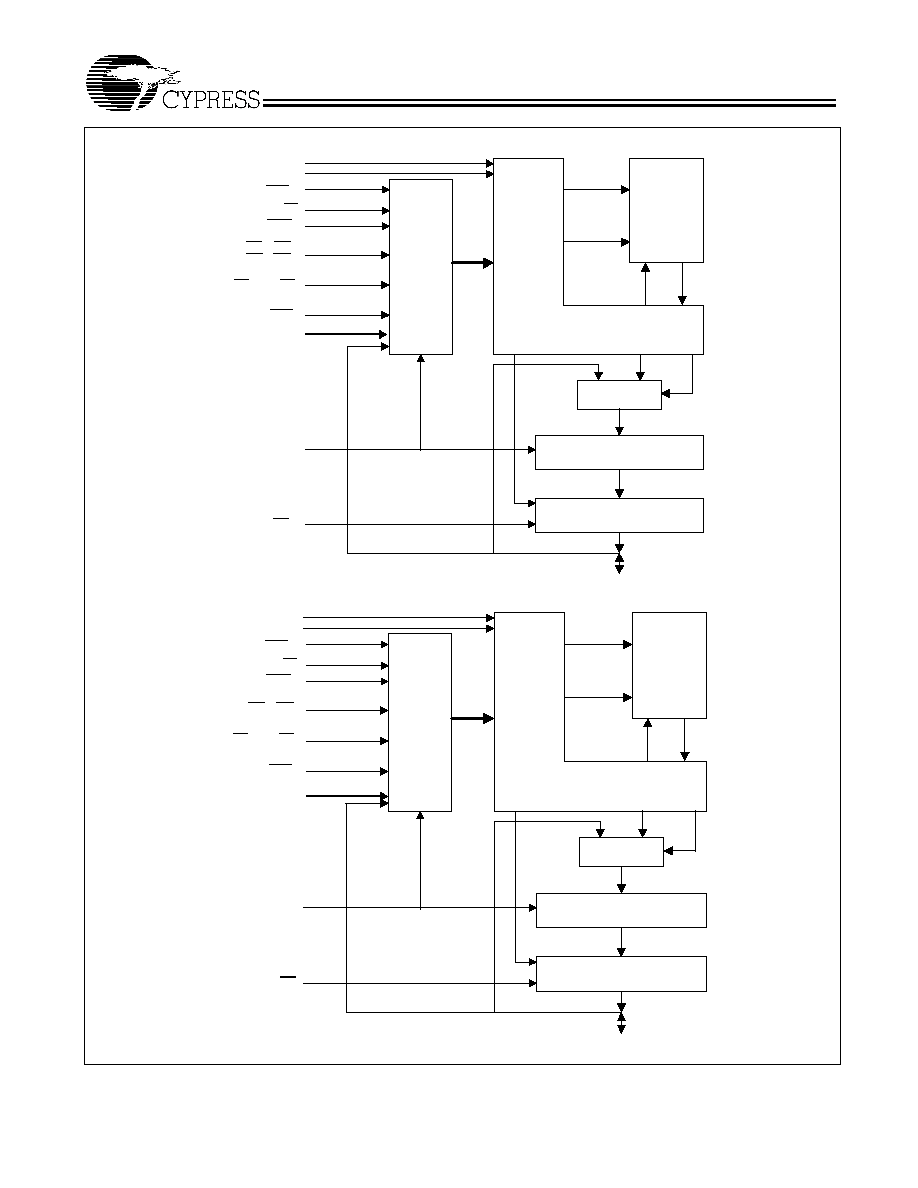
The Functional Block Diagram illustrates simplified device operation. See Truth Table, pin descriptions, and timing diagrams for detailed information.
1M
x 9 x 2
S
RAM Arra
y
DQa, DQb
CLK
Input
Registers
Mux
Output Registers
Output Buffers
Address
Control
DI
DO
Sel
Control Logic
OE#
ZZ
MODE
CKE#
ADV/LD#
R/W#
BWa#, BWb#
CE#, CE2#, CE2
SA0, SA1, SA
OE
CEN
ADV/LD
WEN
BWa, BWb
CE, CE
2
, CE
3
CEN
A0, A1, A
Functional Block Diagram--256K ◊ 36
[1]
256K
x 9 x 4
SRAM
Arra
y
DQa-DQd
CLK
Input
Registers
Mux
Output Registers
Output Buffers
Address
Control
DI
DO
Sel
Control Logic
OE#
ZZ
MODE
CKE#
ADV/LD#
R/W#
BWa#, BWb#
BWc#, BWd#
CE#, CE2#, CE2
SA0, SA1, SA
Functional Block Diagram--512K ◊ 18
[1]
CEN
ADV/LD
WEN
BWa, BWb,
CE, CE
2
, CE
3
CEN
BWc, BWd
OE
Inp
u
t Re
gis
t
e
r
s
A0, A1, A
CY7C1354A/GVT71256ZC36
CY7C1356A/GVT71512ZC18
Document #: 38-05161 Rev. *B
Page 3 of 31
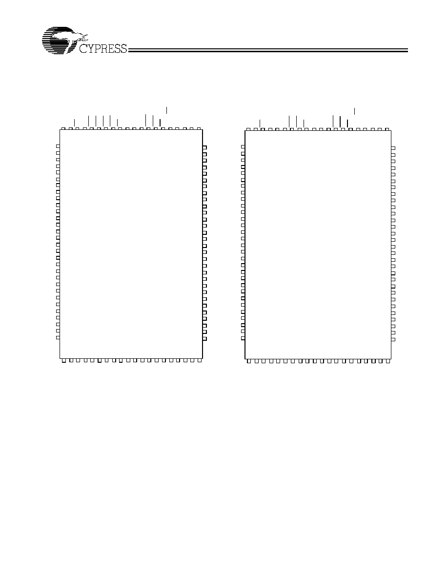
Pin Configurations
A
A
A
A
A1
A0
TM
S
TD
I
V
SS
V
CC
TC
K
A
A
A
A
A
A
V
CCQ
V
SS
DQb
DQb
DQb
V
SS
V
DDQ
DQb
DQb
V
SS
V
CC
V
CC
DQa
DQa
V
CCQ
V
SS
DQa
DQa
V
SS
V
CCQ
V
CCQ
V
SS
DQc
DQc
V
SS
V
CCQ
DQc
DQc
V
CC
V
SS
DQd
DQd
V
CCQ
V
SS
DQd
DQd
DQd
V
SS
V
DDQ
A
A
CE
CE
2
BW
a
CE
3
V
CC
V
SS
CL
K
WE
N
CEN
OE
NC
A
A
1
2
3
4
5
6
7
8
9
10
11
12
13
14
15
16
17
18
19
20
21
22
23
24
25
26
27
28
29
30
31
32
33
34
35
36
37
38
39
40
41
42
43
44
45
46
47
48
49
50
80
79
78
77
76
75
74
73
72
71
70
69
68
67
66
65
64
63
62
61
60
59
58
57
56
55
54
53
52
51
10
0
99
98
97
96
95
94
93
92
91
90
89
88
87
86
85
84
83
82
81
A
A
ADV/L
D
ZZ
TD
O
CY7C1354A/
100-lead TQFP Packages
A
A
A
A
A1
A0
TM
S
TD
I
V
SS
V
CC
TC
K
A
A
A
A
A
A
A
NC
NC
V
CCQ
V
SS
NC
DQa
DQa
DQa
V
SS
V
CCQ
DQa
DQa
V
SS
V
CC
V
CC
DQa
DQa
V
CCQ
V
SS
DQa
DQa
NC
NC
V
SS
V
CCQ
NC
NC
NC
NC
NC
NC
V
CCQ
V
SS
NC
NC
DQb
DQb
V
SS
V
CCQ
DQb
DQb
V
CC
V
SS
DQb
DQb
V
CCQ
V
SS
DQb
DQb
DPb
NC
V
SS
V
CCQ
NC
NC
NC
A
A
CE
CE
2
NC
NC
BW
b
BW
a
CE
3
V
CC
V
SS
CL
K
WE
N
CE
N
OE
NC
A
A
1
2
3
4
5
6
7
8
9
10
11
12
13
14
15
16
17
18
19
20
21
22
23
24
25
26
27
28
29
30
31
32
33
34
35
36
37
38
39
40
41
42
43
44
45
46
47
48
49
50
80
79
78
77
76
75
74
73
72
71
70
69
68
67
66
65
64
63
62
61
60
59
58
57
56
55
54
53
52
51
10
0
99
98
97
96
95
94
93
92
91
90
89
88
87
86
85
84
83
82
81
A
A
AD
V
/
L
D
ZZ
MO
D
E
TD
O
CY7C1356A/
BW
d
MO
D
E
BW
c
DQc
DQc
DQc
DQc
DQc
DQd
DQd
DQd
DQd
DQb
DQb
DQa
DQa
DQa
DQa
DQa
DQb
DQb
(256K ◊ 36)
(512K ◊ 18)
BW
b
V
CC
V
CC
V
CC
GVT71256ZC36
GVT71512ZC18
V
CC

CY7C1354A/GVT71256ZC36
CY7C1356A/GVT71512ZC18
Document #: 38-05161 Rev. *B
Page 4 of 31
Pin Configurations
(continued)
CY7C1354A/GVT71256ZC36 (256K ◊ 36)≠7 ◊ 17 BGA
119-ball Bump BGA
CY7C1356A/GVT71512ZC18 (512K ◊ 18)≠7 ◊ 17 BGA
1
2
3
4
5
6
7
A
V
CCQ
A
A
NC
A
A
V
CCQ
B
NC
CE
2
A
ADV/LD
A
CE
3
NC
C
NC
A
A
V
CC
A
A
NC
D
DQc
DQc
V
SS
NC
V
SS
DQb
DQb
E
DQc
DQc
V
SS
CE
V
SS
DQb
DQb
F
V
CCQ
DQc
V
SS
OE
V
SS
DQb
V
CCQ
G
DQc
DQc
BWc
A
BWb
DQb
DQb
H
DQc
DQc
V
SS
WEN
V
SS
DQb
DQb
J
V
CCQ
V
CC
NC
V
CC
NC
V
CC
V
CCQ
K
DQd
DQd
V
SS
CLK
V
SS
DQa
DQa
L
DQd
DQd
BWd
NC
BWa
DQa
DQa
M
V
CCQ
DQd
V
SS
CEN
V
SS
DQa
V
CCQ
N
DQd
DQd
V
SS
A1
V
SS
DQa
DQa
P
DQd
DQd
V
SS
A0
V
SS
DQa
DQa
R
NC
A
MODE
V
CC
V
SS
A
NC
T
NC
NC
A
A
A
NC
ZZ
U
V
CCQ
TMS
TDI
TCK
TDO
NC
V
CCQ
1
2
3
4
5
6
7
A
V
CCQ
A
A
NC
A
A
V
CCQ
B
NC
CE
2
A
ADV/LD
A
CE
3
NC
C
NC
A
A
V
CC
A
A
NC
D
DQb
NC
V
SS
NC
V
SS
DQa
NC
E
NC
DQb
V
SS
CE
V
SS
NC
DQa
F
V
CCQ
NC
V
SS
OE
V
SS
DQa
V
CCQ
G
NC
DQb
BWb
A
V
SS
NC
DQa
H
DQb
NC
V
SS
WEN
V
SS
DQa
NC
J
V
CCQ
V
CC
NC
V
CC
NC
V
CC
V
CCQ
K
NC
DQb
V
SS
CLK
V
SS
NC
DQa
L
DQb
NC
V
SS
NC
BWa
DQa
NC
M
V
CCQ
DQb
V
SS
CEN
V
SS
NC
V
CCQ
N
DQb
NC
V
SS
A1
V
SS
DQa
NC
P
NC
DQb
V
SS
A0
V
SS
NC
DQa
R
NC
A
MODE
V
CC
V
CC
A
NC
T
NC
A
A
NC
A
A
ZZ
U
V
CCQ
TMS
TDI
TCK
TDO
NC
V
CCQ

CY7C1354A/GVT71256ZC36
CY7C1356A/GVT71512ZC18
Document #: 38-05161 Rev. *B
Page 5 of 31
Pin Descriptions--256K ◊ 36
256K ◊ 36
TQFP Pins
256K ◊ 36
PBGA Pins
Pin
Name
Type
Pin Description
37,
36,
32, 33, 34, 35,
44, 45, 46, 47,
48, 49, 50, 81,
82, 83, 99, 100
4P
4N
2A, 3A, 5A, 6A,
3B, 5B, 2C, 3C,
5C, 6C, 4G, 2R,
6R, 3T, 4T, 5T
A0,
A1,
A
Input-
Synchronous
Synchronous Address Inputs: The address register is triggered by a
combination of the rising edge of CLK, ADV/LD LOW, CEN LOW and
true chip enables. A0 and A1 are the two least significant bits (LSBs) of
the address field and set the internal burst counter if burst cycle is
initiated.
93,
94,
95,
96
5L
5G
3G
3L
BWa,
BWb,
BWc,
BWd
Input-
Synchronous
Synchronous Byte Write Enables: Each nine-bit byte has its own
active LOW byte Write enable. On load Write cycles (when WEN and
ADV/LD are sampled LOW), the appropriate byte Write signal (BWx)
must be valid. The byte Write signal must also be valid on each cycle of
a burst Write. Byte Write signals are ignored when WEN is sampled
HIGH. The appropriate byte(s) of data are written into the device two
cycles later. BWa controls DQa pins; BWb controls DQb pins; BWc
controls DQc pins; BWd controls DQd pins. BWx can all be tied LOW if
always doing Writes to the entire 36-bit word.
87
4M
CEN
Input-
Synchronous
Synchronous Clock Enable Input: When CEN is sampled HIGH, all
other synchronous inputs, including clock are ignored and outputs
remain unchanged. The effect of CEN sampled HIGH on the device
outputs is as if the LOW-to-HIGH clock transition did not occur. For
normal operation, CEN must be sampled LOW at rising edge of clock.
88
4H
WEN
Input-
Synchronous
Read Write: WEN signal is a synchronous input that identifies whether
the current loaded cycle and the subsequent burst cycles initiated by
ADV/LD is a Read or Write operation. The data bus activity for the
current cycle takes place two clock cycles later.
89
4K
CLK
Input-
Synchronous
Clock: This is the clock input to CY7C1354A/GVT71256ZC36. Except
for OE, ZZ and MODE, all timing references for the device are made
with respect to the rising edge of CLK.
98, 92
4E, 6B
CE,
CE
3
Input-
Synchronous
Synchronous Active LOW Chip Enable: CE and CE
3
are used with
CE
2
to enable the CY7C1354A/GVT71256ZC36. CE or CE
3
sampled
HIGH or CE
2
sampled LOW, along with ADV/LD LOW at the rising edge
of clock, initiates a deselect cycle. The data bus will be High-Z two clock
cycles after chip deselect is initiated.
97
2B
CE
2
Input-
Synchronous
Synchronous Active High Chip Enable: CE
2
is used with CE and CE
3
to enable the chip. CE
2
has inverted polarity but otherwise is identical
to CE and CE
3
.
86
4F
OE
Input
Asynchronous Output Enable: OE must be LOW to Read data. When
OE is HIGH, the I/O pins are in high-impedance state. OE does not need
to be actively controlled for Read and Write cycles. In normal operation,
OE can be tied LOW.
85
4B
ADV/
LD
Input-
Synchronous
Advance/Load: ADV/LD is a synchronous input that is used to load the
internal registers with new address and control signals when it is
sampled LOW at the rising edge of clock with the chip is selected. When
ADV/LD is sampled HIGH, then the internal burst counter is advanced
for any burst that was in progress. The external addresses and WEN
are ignored when ADV/LD is sampled HIGH.
31
3R
MOD
E
Input-
Static
Burst Mode: When MODE is HIGH or NC, the interleaved burst
sequence is selected. When MODE is LOW, the linear burst sequence
is selected. MODE is a static DC input.
64
7T
ZZ
Input-
Asynchronous
Sleep Enable: This active HIGH input puts the device in low power
consumption standby mode. For normal operation, this input has to be
either LOW or NC.