IBIS4
1.3 Megapixel CMOS APS
09-Sep-02 12:07
2/41
Overview
The IBIS4 is a digital CMOS active pixel image sensor with SXGA format.
Due to a patented pixel configuration a 60% fill factor and 50% quantum efficiency are obtained. This
is combined with an on-chip double sampling technique to cancel fixed pattern noise.
Main features
∑ SXGA resolution: 1280 x 1024 pixels
∑ High sensitivity 20 µV/electron
∑ High fill factor 60 %
∑ Quantum efficiency > 50% between 500 and 700 nm.
∑ 20 noise electrons = 50 noise photons
∑ Dynamic range: 66 dB (2000:1) in single slope operation
∑ Extended dynamic range mode (80...100 dB) in double slope integration
∑ On-chip 10 bit, 10 mega Samples/s ADC
∑ Programmable gain & offset output amplifier
∑ 4:1 sub sampling viewfinder mode (320x256 pixels)
∑ Electronic shutter
∑ 7 x 7 µm
2
pixels
∑ Low fixed pattern noise (1 % Vsat p/p)
∑ Low dark current: 344 pA/cm
2
(1055 electrons/s, 1 minute auto saturation)
∑ RGB or monochrome
∑ Digital (ADC) gamma correction
Part Number
Color or B/W
Ibis4-1300-M B&W
Ibis4-1300-C1
RGB diagonal stripes
Ibis4-1300-C2
RGB Bayer pattern

IBIS4
1.3 Megapixel CMOS APS
09-Sep-02 12:07
3/41
Table of contents
1
Architecture of the image sensor.........................................................................................................4
1.1
Image sensor core ≠ focal plane array......................................................................................5
1.1.1
Light sensitivity ...................................................................................................................7
1.1.2
Color sensitivity...................................................................................................................9
1.1.3
Charge conversion - Conversion of electrons in an output signal....................................10
1.2
Output amplifier .....................................................................................................................12
1.2.1
Output amplifier offset level adjustment ..........................................................................13
1.2.2
Output amplifier gain control............................................................................................16
1.2.3
Setting of the VLOW_DAC & VHIGH_DAC reference voltages ..................................18
1.3
Analog to digital converter.....................................................................................................18
1.3.1
ADC timing .......................................................................................................................18
1.3.2
Control of the VLOW_ADC & VHIGH_ADC reference voltages .................................21
1.3.3
Non-linear and linear conversion mode ≠ "gamma" correction.......................................21
2
Operation of the image sensor...........................................................................................................22
2.1
Set configuration & pulse timing...........................................................................................22
2.1.1
Set configuration ...............................................................................................................23
2.1.2
Viewfinder mode vs. normal readout................................................................................23
2.1.3
Start of the Y shift registers for row readout & row reset ................................................23
2.1.4
End-of-scan: EOS_YL, EOS_YR, EOS_X ......................................................................24
2.1.5
Row initialization ..............................................................................................................24
2.1.6
The X-direction shift register ............................................................................................27
2.1.7
Pixel readout ......................................................................................................................28
2.1.8
Example: timing used on the IBIS4 breadboard...............................................................28
2.2
Illumination control................................................................................................................29
2.2.1
"Rolling curtain" electronic shutter ..................................................................................29
2.2.2
Gain control .......................................................................................................................29
2.2.3
Offset level adjustment......................................................................................................30
2.3
"Double slope" or "High-dynamic range" mode ...................................................................30
2.4
Electrical parameters ..............................................................................................................32
2.4.1
DC voltages .......................................................................................................................32
2.4.2
Input / output .....................................................................................................................32
3
Pin configuration................................................................................................................................33
3.1
Pin list .....................................................................................................................................33
3.2
Bonding pad geometry for the IBIS4.....................................................................................36
3.2.1
Color filter geometry .........................................................................................................36
4
Package ..............................................................................................................................................37
4.1
Cover glass .............................................................................................................................38
4.1.1
Color sensor.......................................................................................................................38
4.1.2
Monochrome sensor ..........................................................................................................39
5
FAQ ≠ Application notes...................................................................................................................40
5.1
Temperature dependence of dark signal ................................................................................40

IBIS4
1.3 Megapixel CMOS APS
09-Sep-02 12:07
5/41
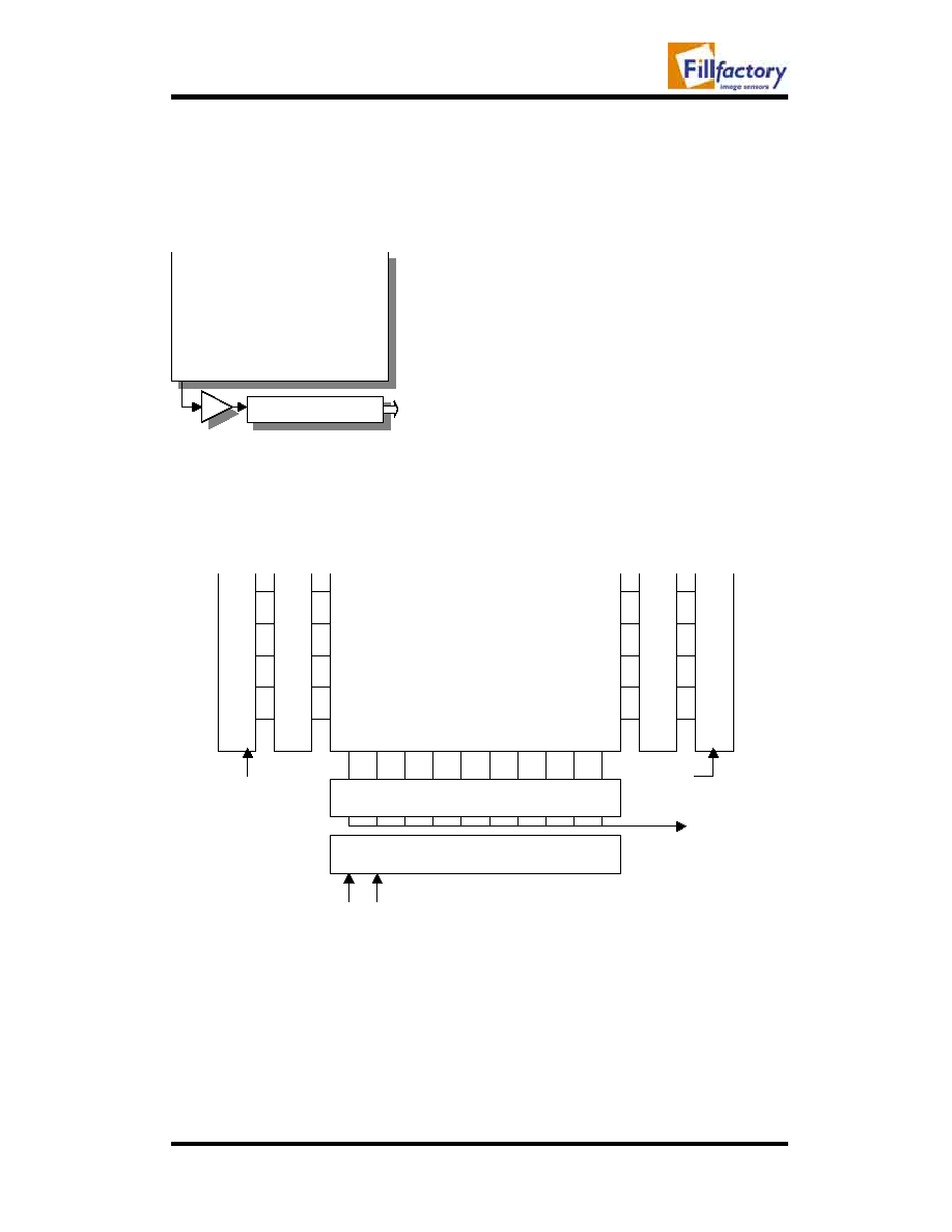
1.1 Image sensor core ≠ focal plane array
Figure 1 shows the architecture of the image sensor core.
The core of the sensor is the pixel array with 1280 x 1024 (SXGA) active pixels.
The name `active pixels' refers to the amplifying element in each pixel. This type of pixels offer a high
light sensitivity combined with low temporal noise. The actual array size is 1286 x 1030 including the 6
dummy pixels in X and Y. Although the dummy pixels fall outside the SXGA format, their information
can be used e.g. for color filter array interpolation.
Y
re
ad
o
u
t sh
i
f
t re
gi
st
e
r
X shift register
Figure 2: Pixel selection - principle
Next to the pixel array there are two Y shift registers, and one X shift register with the column
amplifiers. The shift registers act as pointers to a certain row or column. The Y readout shift register
accesses the row (line) of pixels that is currently readout. The X shift register selects a particular pixel
of this row. The second Y shift register is used to point at the row of pixels that is reset. The delay
between both Y row pointers determines the integration time -thus realizing the electronic shutter.
A clock and a synchronization pulse control the shift registers. On every clock pulse, the pointer shifts
one row/column further. A sync pulse is used to reset and initialize the shift registers to their first
position.
The smart column amplifiers compensate the offset variations between individual pixels. To do so, they
need a specific pulse pattern on specific control signals before the start of the row readout.
Table 1 summarizes the optical and electrical characteristics of the image sensor. Some specifications
are influenced by the output amplifier gain setting (e.g. temporal noise, conversion factor,...).
Therefore, all specifications are referred to an output amplifier gain equal to 1.
Table 1: optical & electrical characteristics