Spread Spectrum Clock Generator
SM560
Cypress Semiconductor Corporation
∑
3901 North First Street
∑
San Jose
∑
CA 95134
∑
408-943-2600
Document #: 38-07020 Rev. *C
Revised December 14, 2002
Features
∑ 25- to 108-MHz operating frequency range
∑ Wide (9) range of spread selections
∑ Accepts clock and crystal inputs
∑ Low power dissipation
∑ 3.3V = 85 mw (50 MHz)
∑ Frequency Spread disable function
∑ Center Spread modulation
∑ Low cycle-to cycle jitter
∑ Eight-pin SOIC package
Applications
∑ VGA controllers
∑ LCD panels and monitors
∑ Printers and multi-function devices (MFP)
Benefits
∑ Peak electromagnetic interference (EMI) reduction
by 8 to 16 dB
∑ Fast time to market
∑ Cost reduction
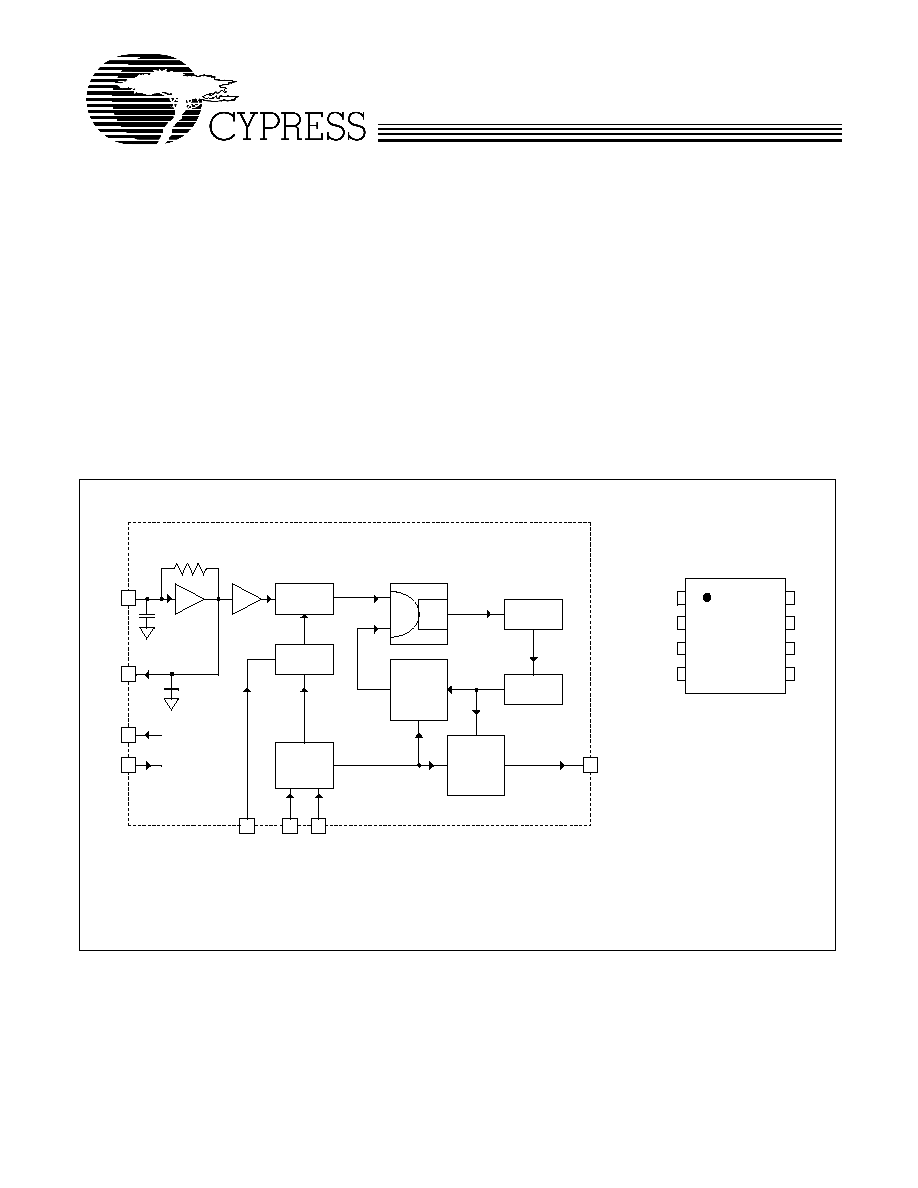
Block Diagram
Pin Configuration
PD
VCO
1
8
Xin/
CLK
Xout
REFERENCE
DIVIDER
4 pf
8 pF
250 K
FEEDBACK
DIVIDER
MODULATION
CONTROL
DIVIDER
AND MUX
5
2
3
7
VDD
SSCC
SSCLK
VSS
4
6
LF
INPUT
DECODER
LOGIC
S1
S0
CP
1
2
3
4
8
7
6
5
Xin/CLK
VDD
SSCLK
VSS
Xout
S0
S1
SSCC
S
M
560
SM560
Document #: 38-07020 Rev. *C
Page 2 of 8
General Description
The Cypress SM560 is a Spread Spectrum Clock Generator
(SSCG) IC used for the purpose of reducing Electro Magnetic
Interference (EMI) found in today's high-speed digital
electronic systems.
The SM560 uses a Cypress-proprietary Phase-Locked Loop
(PLL) and Spread Spectrum Clock (SSC) technology to
synthesize and frequency modulate the input frequency of the
reference clock. By frequency modulating the clock, the
measured EMI at the fundamental and harmonic frequencies
of Clock (SSCLK1) is greatly reduced.
This reduction in radiated energy can significantly reduce the
cost of complying with regulatory requirements and time to
market without degrading the system performance.
The SM560 is a very simple and versatile device to use. The
frequency and spread% range is selected by programming S0
and S1digital inputs. These inputs use three (3) logic states
including High (H), Low (L) and Middle (M) logic levels to select
one of the nine available Frequency Modulation and Spread%
ranges. Refer to Table 1 for programming details.
The SM560 is optimized for SVGA (40 MHz) and XVGA (65
MHz) Controller clocks and also suitable for the applications
with the frequency range of 25 to 108 MHz.
A wide range of digitally selectable spread percentages is
made possible by using three-level (High, Low and Middle)
logic at the S0 and S1 digital control inputs.
The output spread (frequency modulation) is symmetrically
centered on the input frequency.
Spread Spectrum Clock Control (SSCC) function enables or
disables the frequency spread and is provided for easy
comparison of system performance during EMI testing.
The SM560 is available in an eight-pin SOIC package with a 0
to 70
∞
C operating temperature range.
Pin Description
Pin
Name
Type
Description
1
Xin/CLK
I
Clock or Crystal connection input. Refer to Table 1 for input frequency range selection.
2
VDD
P
Positive power supply.
3
GND
P
Power supply ground.
4
SSCLK
O
Modulated clock output.
5
SSCC
I
Spread Spectrum Clock Control (Enable/Disable) function. SSCG function is enabled
when input is high and disabled when input is low. This pin is pulled high internally.
6
S1
I
Tri-level Logic input control pin used to select frequency and bandwidth.
Frequency/bandwidth selection and Tri-level Logic programming. See Figure 1.
7
S0
I
Tri-level Logic input control pin used to select frequency and bandwidth.
Frequency/bandwidth selection and Tri-level Logic programming. See Figure 1.
8
Xout
O
Oscillator output pin connected to crystal. Leave this pin unconnected If an external
clock drives Xin/CLK.
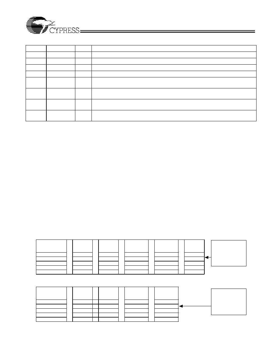
Table 1. Frequency and Spread% Selection (Center Spread)
2 5 ≠ 5 4 M H z (L o w R a n g e )
In p u t
F re q u e n c y
(M H z )
S 1 = M
S 0 = M
(% )
S 1 = M
S 0 = 0
(% )
S 1 = 1
S 0 = 0
(% )
S 1 = 0
S 0 = 0
(% )
S 1 = 0
S 0 = M
(% )
2 5 ≠ 3 5
3 .8 3 .2 2 .8 2 .3 1 .9
3 5 ≠ 4 0
3 .5 3 .0 2 .5 2 .1 1 .7
4 0 ≠ 4 5
3 .2 2 .8 2 .4 1 .9 1 .6
4 5 ≠ 5 0
3 .0 2 .6 2 .2 1 .8 1 .5
5 0 ≠ 5 4
2 .8 2 .4 2 .0 1 .7 1 .4
5 0 ≠ 1 0 8 M H z (H ig h R a n g e )
In p u t
F re q u e n c y
(M H z )
S 1 = 1
S 0 = M
(% )
S 1 = 0
S 0 = 1
(% )
S 1 = 1
S 0 = 1
(% )
S 1 = M
S 0 = 1
(% )
5 0 ≠ 6 0
2 .5 1 .9 1 .2 1 .0
6 0 ≠ 7 0
2 .4 1 .8 1 .1 0 .9
7 0 ≠ 8 0
2 .3 1 .6 1 .1 0 .9
8 0 ≠ 1 0 0
2 .0 1 .4 1 .0 0 .8
1 0 0 ≠ 1 0 8
1 .8 1 .3 0 .8 0 .6
S e le c t th e
F re q u e n c y a n d
C e n te r S p re a d %
d e s ir e d a n d th en
s e t S 1 , S 0 a s
in d ic a te d .
S e le c t th e
F re q u e n c y a n d
C e n te r S p re a d %
d e s ir e d a n d th en
s e t S 1 , S 0 a s
in d ic a te d .
SM560
Document #: 38-07020 Rev. *C
Page 3 of 8
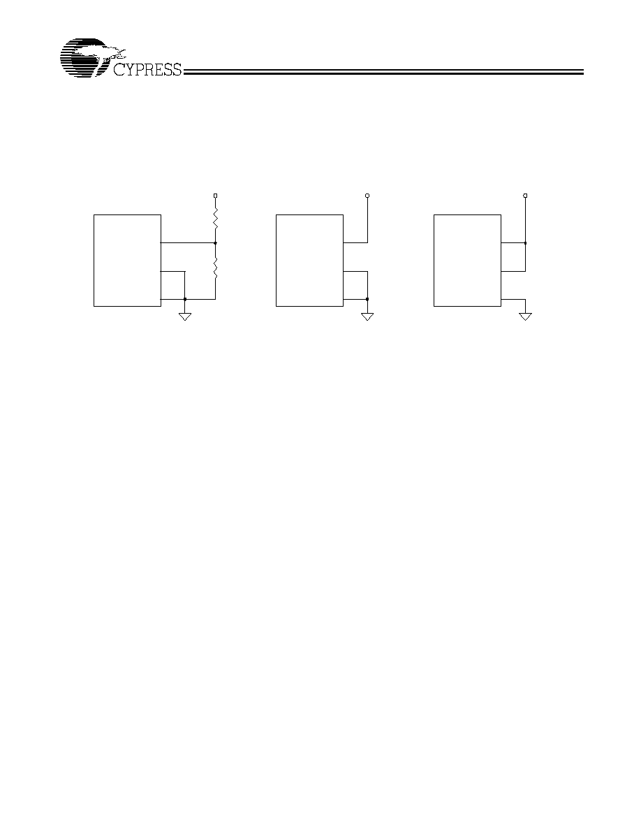
Tri-level Logic
With binary logic, four states can be programmed with two
control lines, whereas Tri-level Logic can program nine logic
states using two control lines. Tri-level Logic in the SM560 is
implemented by defining a third logic state in addition to the
standard logic "1" and "0." Pins 6 and 7 of the SM560
recognize a logic state by the voltage applied to the respective
pin. These states are defined as "0" (Low), "M" (Middle), and
"1" (One). Each of these states has a defined voltage range
that is interpreted by the SM560 as a "0," "M," or "1" logic state.
Refer to Table 2 for voltage ranges for each logic state. By
using two equal value resistors (typically 20K) the "M" state
can be easily programmed. Pins 6 or 7 can be tied directly to
ground or VDD for Logic "0" or "1" respectively..
VDD = 3.3 VDC
VDD = 3.3 VDC
VDD = 3.3 VDC
SM560
5
6
7
7
6
5
SM560
1.65 VDC
0 VDC
SM560
7
6
5
EX. 1
EX. 2
EX. 3
20K
20K
Figure 1.
SM560
Document #: 38-07020 Rev. *C
Page 4 of 8
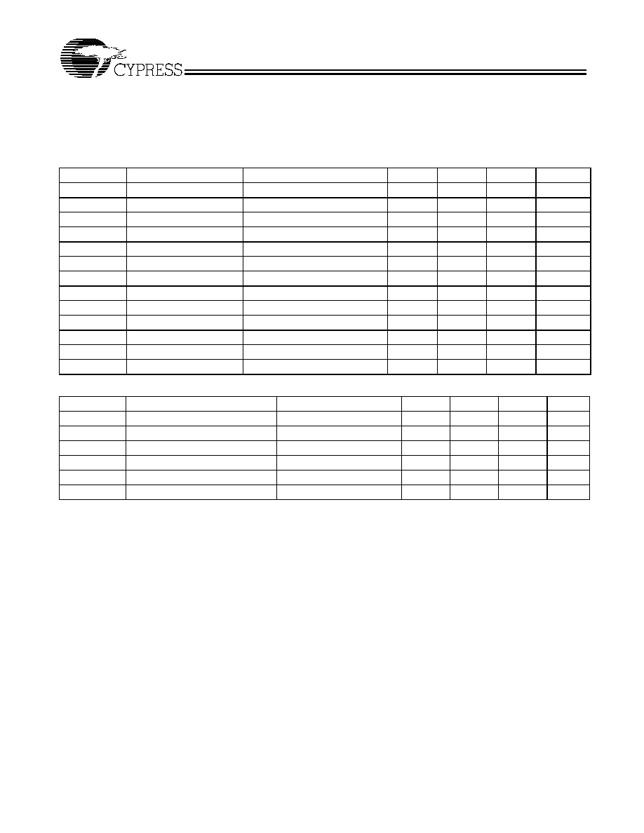
Absolute Maximum Ratings
[1]
Supply Voltage (V
DD
): .................................... ≠0.5V to +6.0V
DC Input Voltage: ..................................≠0.5V to VDD + 0.5V
Junction Temperature .................................≠40∞C to +140∞C
Operating Temperature:...................................... 0∞C to 70∞C
Storage Temperature .................................. ≠65∞C to +150∞C
Static Discharge Voltage (ESD)........................... 2,000V-Min
SSCG Theory of Operation
The SM560 is a PLL-type clock generator using a proprietary
Cypress design. By precisely controlling the bandwidth of the
output clock, the SM560 becomes a Low EMI clock generator.
The theory and detailed operation of the SM560 will be
discussed in the following sections.
EMI
All digital clocks generate unwanted energy in their harmonics.
Conventional digital clocks are square waves with a duty cycle
that is very close to 50%. Because of this 50/50-duty cycle,
digital clocks generate most of their harmonic energy in the
odd harmonics, i.e.; third, fifth, seventh, etc. It is possible to
reduce the amount of energy contained in the fundamental
and odd harmonics by increasing the bandwidth of the funda-
mental clock frequency. Conventional digital clocks have a
very high Q factor, which means that all of the energy at that
frequency is concentrated in a very narrow bandwidth, conse-
quently, higher energy peaks. Regulatory agencies test
electronic equipment by the amount of peak energy radiated
from the equipment. By reducing the peak energy at the funda-
mental and harmonic frequencies, the equipment under test is
able to satisfy agency requirements for EMI. Conventional
methods of reducing EMI have been to use shielding, filtering,
multi-layer PCBs, etc. The SM560 uses the approach of
reducing the peak energy in the clock by increasing the clock
bandwidth, and lowering the Q.
SSCG
SSCG uses a patented technology of modulating the clock
over a very narrow bandwidth and controlled rate of change,
both peak and cycle to cycle. The SM560 takes a narrow band
digital reference clock in the range of 25≠108 MHz and
produces a clock that sweeps between a controlled start and
stop frequency and precise rate of change. To understand
what happens to a clock when SSCG is applied, consider a
65-MHz clock with a 50% duty cycle. From a 65-MHz clock we
know the following:
Note:
1.
Single Power Supply: The Voltage on any input or I/O pin cannot exceed the power pin during power up.
Table 2. DC Electrical Characteristics: V
DD
= 3.3V, Temp. = 25∞C and C
L
(Pin 4) = 15 pF, unless otherwise noted
Parameter
Description
Conditions
Min.
Typ.
Max.
Unit
V
DD
Power Supply Range
±10%
2.97
3.3
3.63
V
V
INH
Input High Voltage
S0 and S1 only
0.85V
DD
V
DD
V
DD
V
V
INM
Input Middle Voltage
S0 and S1 only
0.40V
DD
0.50V
DD
0.60V
DD
V
V
INL
Input Low Voltage
S0 and S1 only
0.0
0.0
0.15V
DD
V
V
OH1
Output High Voltage
I
OH
= 6 mA
2.4
V
V
OH2
Output High Voltage
I
OH
= 20 mA
2.0
V
V
OL1
Output Low Voltage
I
OH
= 6 mA
0.4
V
V
OL2
Output Low Voltage
I
OH
= 20 mA
1.2
V
Cin1
Input Capacitance
Xin/CLK (Pin 1)
3
4
5
pF
Cin2
Input Capacitance
Xout (Pin 8)
6
8
10
pF
Cin2
Input Capacitance
S0, S1, SSCC (Pins 7,6,5)
3
4
5
pF
I
DD1
Power Supply Current
F
IN
= 40 MHz
30
40
mA
I
DD2
Power Supply Current
F
IN
= 65 MHz
35
45
mA
Table 3. Electrical Timing Characteristics: V
DD
= 3.3V, T = 25∞C and C
L
= 15 pF, unless otherwise noted
Parameter
Description
Conditions
Min.
Typ.
Max.
Unit
ICLKFR
Input Clock Frequency Range
V
DD
= 3.30V
25
108
MHz
Trise
Clock Rise Time (Pin 4)
SSCLK1 @ 0.4 ≠ 2.4V
1.2
1.4
1.6
ns
Tfall
Clock Fall Time (Pin 4)
SSCLK1 @ 0.4 ≠ 2.4V
1.2
1.4
1.6
ns
DTYin
Input Clock Duty Cycle
XIN/CLK (Pin 1)
20
50
80
%
DTYout
Output Clock Duty Cycle
SSCLK1 (Pin 4)
45
50
55
%
JCC
Cycle-to-Cycle Jitter
Fin = 25 ≠ 108 MHz
-
125
175
ps
SM560
Document #: 38-07020 Rev. *C
Page 5 of 8
If this clock is applied to the Xin/CLK pin of the SM560, the
output clock at pin 4 (SSCLK) will be sweeping back and forth
between two frequencies. These two frequencies, F1 and F2,
are used to calculate to total amount of spread or bandwidth
applied to the reference clock at pin 1. As the clock is making
the transition from f1 to f2, the amount of time and sweep
waveform play a very important role in the amount of EMI
reduction realized from an SSCG clock.
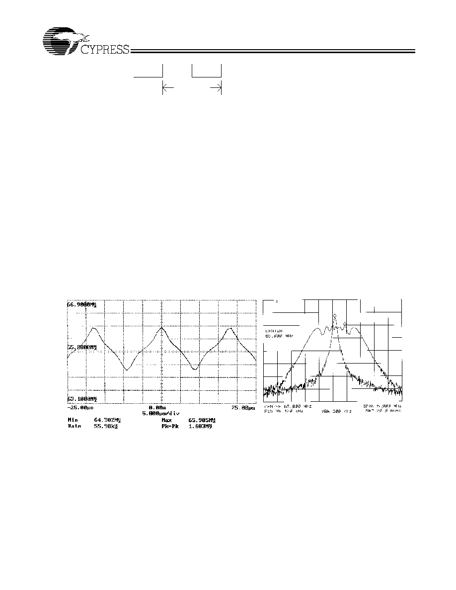
The modulation domain analyzer is used to visualize the
sweep waveform and sweep period. The left side of Figure 2
shows the modulation profile of a 65-MHz SSCG clock. Notice
that the actual sweep waveform is not a simple sine or
sawtooth waveform. The right side of Figure 2 is a scan of the
same SSCG clock using a spectrum analyzer. In this scan you
can see a 6.48-dB reduction in the peak RF energy when using
the SSCG clock.
Modulation Rate
Spectrum Spread Clock Generators utilize frequency
modulation (FM) to distribute energy over a specific band of
frequencies. The maximum frequency of the clock (Fmax) and
minimum frequency of the clock (Fmin) determine this band of
frequencies. The time required to transition from Fmin to Fmax
and back to Fmin is the period of the Modulation Rate, Tmr.
Modulation Rates of SSCG clocks are generally referred to in
terms of frequency or Fmod = 1/Tmod.
The input clock frequency, Fin, and the internal divider count,
Cdiv, determine the Modulation Rate. In some SSCG clock
generators, the selected range determines the internal divider
count. In other SSCG clocks, the internal divider count is fixed
over the operating range of the part. The SM560 and SM561
have a fixed divider count, as listed below.
Tc = 15.4 ns
50 %
50 %
lock Frequency = fc = 65MHz
lock Period = Tc =1/65 MHz = 15.4 ns
Device
Cdiv
SM560
1166
(All
Ranges)
SM561
2332
(All Ranges)
Example:
Device
=
SM560
Fin
=
65
MHz
Range =
S1 = 1, S0 = M
Then;
Modulation Rate = Fmod = 65 MHz/1166 = 55.8 kHz.
Modulation Profile
Spectrum Analyzer
BW = 2.46%
Figure 2. SSCG Clock, SM560, Fin = 65 MHz