
Spread Spectrum Clock Generator
Cypress Semiconductor Corporation
525 Los Coches St.
Document#: 38-07023 Rev. *A
12/14/02
Milpitas, CA 95035. Tel: 408-263-6300, Fax: 408-263-6571
Page 1 of 11
http://www.cypress.com
SM566
FEATURES
∑
25 to 200 MHz Operating Frequency Range
∑
Wide (9) Range of Spread Selection
∑
Accepts Clock and Crystal Inputs
∑
Provides 4 clocks
(SSCLK1A, SSCLK1b, SSCLK2, REFOUT)
∑
Low
Power
Dissipation
3.3V = 85 mw. (Typical @ 40 MHz, No Load.)
∑
Center Spread Modulation
∑
Low Cycle-to Cycle Jitter
∑
Available in 16-pin (150 mil.) SOIC package
APPLICATIONS
∑
SVGA and XVGA Controllers
∑
LCD Panels and Monitors
∑
Printers
and
MFPs
BENEFITS
∑
Peak EMI reduction by 8 to 16dB
∑
Fast Time to Market
∑
Cost
Reduction
GENERAL DESCRIPTION
The CYPRESS SM566 is a Spread Spectrum Clock Generator (SSCG) IC used for the purpose of reducing Electro
Magnetic Interference (EMI) found in today's high-speed digital electronic systems.
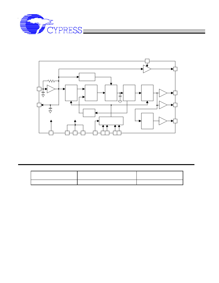
The SM566 uses a Cypress proprietary Phase-Locked Loop (PLL) and Spread Spectrum Clock (SSC) technology
to synthesize and frequency modulate the input frequency of the digital clock. By frequency modulating the clock,
(SSCLK1a/b and SSCLK2), the measured EMI at the fundamental and harmonic frequencies is greatly reduced.
The modulated output frequency is centered on the input frequency.
This reduction in radiated energy can significantly reduce the cost of complying with regulatory agency
requirements and improve time to market without degrading system performance.
The SM566 provides 4 output clocks, SSCLK1a, SSCLK1b, SSCLK2 and REFOUT. SSCLK1a/b and SSCLK2 are
modulated clocks and REFOUT is a buffered copy of the reference clock or oscillator. The SM566 frequency and
spread % ranges are selected by programming S0, S1, S2 and S3 digital inputs. S0 and S1 use three (3) logic
states including High (H), Low (L) and Middle (M) logic levels to select one of 9 available Frequency and Spread %
ranges. Refer to page 6 for details on programming Tri-Level inputs S0 and S1. Programming details for S2 and
S3 can be found on pages 6 and 8.
The SM566 will operate over a wide range of frequencies from 25 to 200 MHz. Operation to 200 MHz is possible
with the use of Dual Drivers at pins 8 and 9. With a wide range of selectable bandwidths, the SM566 is a very
flexible Low EMI clock. Modulation can be disabled to provide a 4 output conventional clock.
REFOUT can be used as a baseline comparison when making dB reduction measurements of the modulated clock
outputs, SSCLK1a and/or SSCLK1b.
The SM566 is available in a 16 pin SOIC (150-mil.) package with a commercial operating temperature range of 0 to
70
∞
C.
Spread Spectrum Clock Generator
Cypress Semiconductor Corporation
525 Los Coches St.
Document#: 38-07023 Rev. *A
12/14/02
Milpitas, CA 95035. Tel: 408-263-6300, Fax: 408-263-6571
Page 2 of 11
http://www.cypress.com
SM566
BLOCK DIAGRAM
Figure 1. Block Diagram
ORDERING INFORMATION
Part No.
Package
Operating
Temperature Range
SM566BZ
16 Pin SOIC
0 to 70
∞
C
Table 1. Ordering Information
PHASE
DET.
CHARGE
PUMP
VCO
OUTPUT
DIVIDER
"N" DIVIDER
REF.
DIVIDER
DAC
CONTROL
CONTROL
LOGIC
S0
S2 S3
S1
DIVIDE
BY 2
1
16
4
14
6
13 12
15
8
2
REFOUT
7
REFOFF
SSCLK1a
SSCLK2
3
XIN/CLKIN
XOUT
SSCC
VSS
VSS
5
SSCLK1b
9
11
VDD
10
VSS
4 pF
8 pF
250 K
OSC.
Spread Spectrum Clock Generator
Cypress Semiconductor Corporation
525 Los Coches St.
Document#: 38-07023 Rev. *A
12/14/02
Milpitas, CA 95035. Tel: 408-263-6300, Fax: 408-263-6571
Page 3 of 11
http://www.cypress.com
SM566
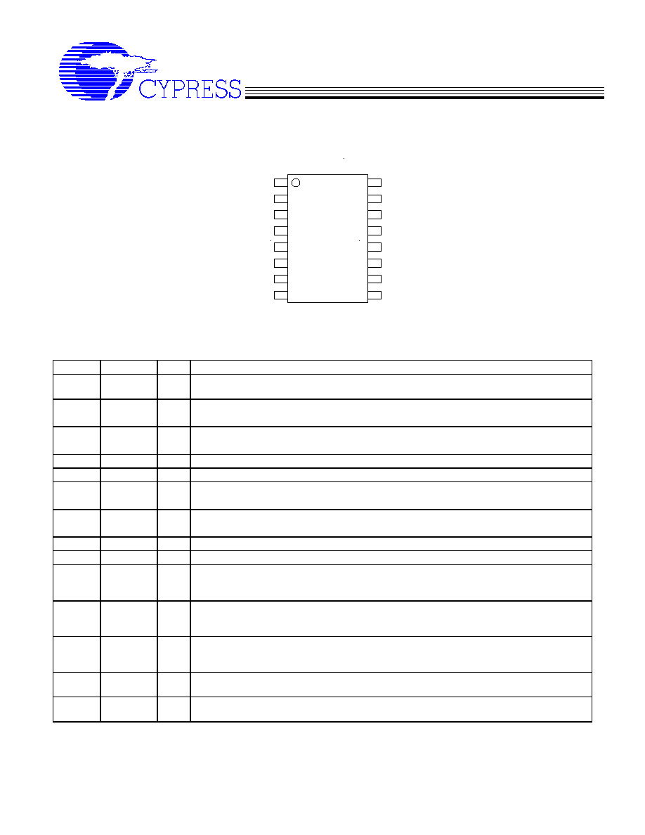
PIN CONFIGURATION
Figure 2. 16 Pin SOIC Pin Assignment
PIN DESCRIPTION
Pin #
Symbol
Type Description
1
Xin/CLKIN
I
Clock or Crystal connection input. Refer to the Table-5, 6 or 7 (page 8) for input frequency
range selection.
2
REFOFF
I
Input pin enables REFOUT clock at pin 3. REFOFF has 400K
internal pull-up resistor.
Logic "0" enables REFOUT, logic "1" disables REFOUT. Default = Disabled.
3
REFOUT
O
Buffered, non-modulated output clock derived from XIN/CLKIN input frequency.
There is a 180
∞
phase shift from XIN to REFOUT.
4
VDD
P
Positive power supply. Bypass to ground with 0.1-uF capacitor.
5, 11, 14
VSS
G
Power supply ground.
6
S2
I
VCO Range control. Refer to page 8 for detailed programming information.
Has 400K
internal pull-up to VDD.
7
S3
I
VCO Range control. Refer to page 8 for detailed programming information.
Has 400K
internal pull-up to VDD.
8
SSCLK1a
O
Modulated clock output. Pins 8 and 9 are identical but separate drivers.
9
SSCLK1b
O
Modulated clock output. Pins 8 and 9 are identical but separate drivers.
10
SSCC
I
Spread Spectrum Clock Control (Enable/Disable) function. SSCG function is enabled when
input is high and disabled when input is low. Internal 400K
pull-up defaults to modulation
ON.
12
S1
I
Tri-Level Logic input control pin used to select Frequency and Bandwidth. Refer to Page 8 for
Frequency/Bandwidth selection. Tri-Level Logic programming details can be found on page
6.
13
S0
I
Tri-Level Logic input control pin used to select Frequency and Bandwidth. Refer to Page 8 for
Frequency/Bandwidth selection. Tri-Level Logic programming details can be found on page
6.
15
SSCLK2
O
Modulated output clock. Frequency of SSCLK2 = SSCLK1a/2. BW % of SSCLK2 is equal to
BW % of SSCLK1a/b.
16
XOUT
O
Oscillator output pin connected to crystal. Leave this pin unconnected If an external clock
drives Xin/CLK.
Table 2. Pin Description
1
2
3
4
5
6
8
10
11
12
13
14
15
7
XIN/CLKIN
REFOFF
REFOUT
VDD
VSS
S2
S3
SSCC
VSS
S1
S0
VSS
SSCLK2
XOUT
SSCLK1b
16
SSCLK1a
9
Spread Spectrum Clock Generator
Cypress Semiconductor Corporation
525 Los Coches St.
Document#: 38-07023 Rev. *A
12/14/02
Milpitas, CA 95035. Tel: 408-263-6300, Fax: 408-263-6571
Page 4 of 11
http://www.cypress.com
SM566
ABSOLUTE MAXIMUM RATINGS
1
:
1
Note: Single Power Supply: The Voltage on any input or I/O pin cannot exceed the power pin during power-up.
Supply Voltage (AVDD or DVDD): +6V
AVDD - DVDD: +/-300mV
AGND - DGND: +/-300mV
Operating Temperature: 0 to 70
∞
C
Storage Temperature: -65 to +150
∞
C
Junction Temperature (10-sec. soldering): +300
∞
C
DC ELECTRICAL CHARACTERISTICS:
Test Conditions: VDD=3.3V, T=25
∞
, unless otherwise noted.
Symbol
Parameter
Min.
Typ.
Max.
Unit
Conditions
VDD
Power Supply Range
2.97
3.3
3.63
V
+/- 10 %
VINH
Input High Voltage
0.85VDD
VDD
VDD
V
S0 and S1 only.
VINM
Input Middle Voltage
0.40VDD 0.50VDD 0.60VDD
V
S0 and S1 only.
VINL
Input Low Voltage
0.0
0.0
0.15VDD
V
S0 and S1 only.
VOH1
Output High Voltage
2.4
-
-
V
IOH = 6 ma, SSCLKa
VOH2
Output High Voltage
2.0
-
-
V
IOH = 20 ma, SSCLKb
VOL1
Output Low Voltage
-
-
0.4
V
IOH = 6 ma, SSCLKa
VOL2
Output Low Voltage
-
-
1.2
V
IOH = 20 ma, SSCLKb
Cin1
Input Capacitance
3
4
5
pF
Xin/CLK (Pin 1)
Cin2
Input Capacitance
6
8
10
pF
Xout (Pin 16)
Cin2
Input Capacitance
3
4
5
pF
All input pins except 1.
IDD1
Power Supply Current
-
27
32
ma
FIN = 40 MHz, 15pf @ all outputs.
IDD1
Power Supply Current
-
23
28
ma
FIN = 40 MHz, No Load
IDD2
Power Supply Current
-
50
58
ma
FIN = 165 MHz,15pf @ all outputs.
IDD2
Power Supply Current
-
39
46
ma
FIN = 165 MHz, No Load
Table 3.
TIMING ELECTRICAL CHARACTERISTICS:
Test Conditions: VDD=3.3V, T=25
∞
C, CL=15pF. Rise/Fall time @ 0.4 and 2.4V, duty cycle at 1.5 V. Mod. ON.
Symbol
Parameter
Min.
Typ. Max. Unit Conditions
ICLKFR
Input Frequency Range
27
200
MHz Non crystal, 3.0 volts Pk-Pk. Ext. source.
trise(a)
Clock Rise Time
1.2
1.4
1.6
ns
SSCLK1a or SSCLK1b, Freq. = 100 MHz
tfall(a)
Clock Fall Time
1.2
1.4
1.6
ns
SSCLK1a or SSCLK1b, Freq. = 100 MHz
trise(a+b)
Clock Rise Time
1.3
1.5
1.7
ns
SSCLK1 (a+b), CL = 33 pF, 100 MHz
tfall(a+b)
Clock Fall Time
1.3
1.5
1.7
ns
SSCLK1 (a+b), CL = 33 pF, 100 MHz
trise(a+b)
Clock Rise Time
1.4
1.6
1.8
ns
SSCLK1 (a+b), CL = 33 pF, 200 MHz
tfall(a+b)
Clock Fall Time
1.4
1.6
1.8
ns
SSCLK1 (a+b), CL = 33 pF, 200 MHz
trise(2)
Clock Rise Time
1.1
1.3
1.5
ns
SSCLK2, Pin 15, CL = 15 pF, 12.5 MHz
tfall(2)
Clock Fall Time
1.2
1.4
1.6
ns
SSCLK2, Pin 15, CL = 15 pF, 12.5 MHz
trise(REF)
Clock Rise Time
1.3
1.5
1.7
ns
REFOUT, Pin 3, CL = 15 pF, 65 MHz
tfall(REF)
Clock Fall Time
1.6
1.8
2.0
ns
REFOUT, Pin 3, CL = 15 pF, 65 MHz
Spread Spectrum Clock Generator
Cypress Semiconductor Corporation
525 Los Coches St.
Document#: 38-07023 Rev. *A
12/14/02
Milpitas, CA 95035. Tel: 408-263-6300, Fax: 408-263-6571
Page 5 of 11
http://www.cypress.com
SM566
DTYin
Input Clock Duty Cycle
20
50
80
%
XIN/CLK (Pin 1)
DTYout
Output Clock Duty Cycle
45
50
55
%
SSCLK1a/SSCLKb (Pin 8 and 9)
CCJ
Cycle-to-Cycle Jitter
-
200
225
ps
F = 100 MHz, SSCLK1a/1b CL = 33 pF
CCJ
Cycle-to-Cycle Jitter
-
325
350
ps
F = 200 MHz, SSCLK1a/1b CL = 33 pF
Table 4.
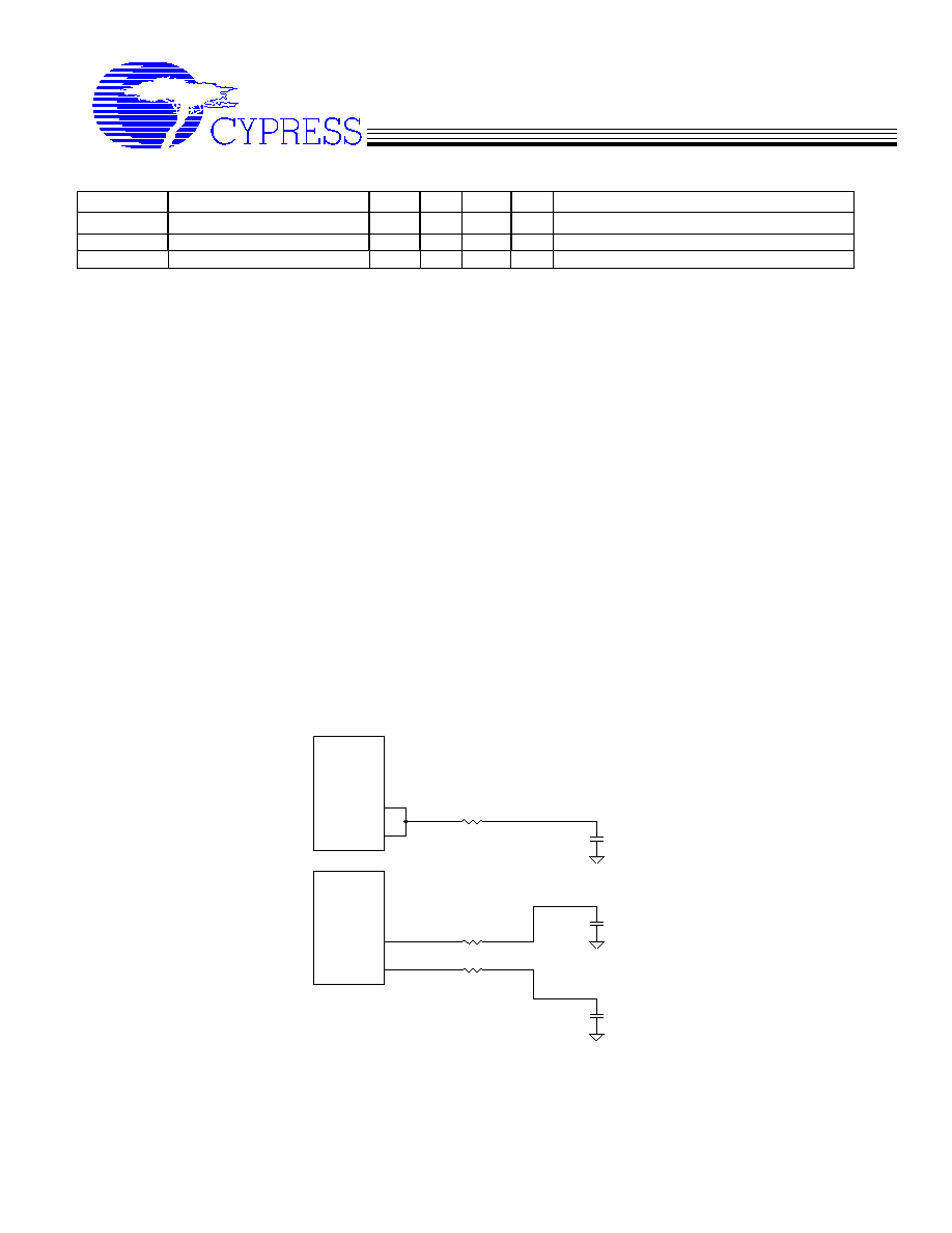
Output Clock Architecture
The SM566 provides 4 separate output clocks, REFOUT, SSCLK1a, SSCLK1b and SSCLK2, for use in a wide
variety of applications. Each clock output is described below in detail.
REFOUT
REFOUT is a 3.3-volt CMOS level non-modulated inverted copy of the clock at XIN/CLKIN. As an inverted clock,
the output clock at REFOUT is 180 degrees out of phase with the input clock at XIN/CLK. Placing a high (1) logic
state on REFOFF, pin 2, will disable the REFOUT clock. When REFOUT is disabled, REFOUT, pin 3, is at a high
(1) logic state.
SSCLK1a/b
SSCLK1a and SSCLK1b are Spread Spectrum clock outputs used for the purpose of reducing EMI in digital
systems. SSCLK1a and SSCLK1b can be connected in several different ways to provide flexibility in application
designs. Each clock can drive separate nets with a capacitive load of up to 15 pF each or connected together to
provide drive to a single net with a capacitive load as high as 33 pF. When both clocks are connected together,
the SM566 is capable of driving 3.3 volt CMOS compatible clocks to frequencies as high as 200 MHz. If one
clock output is not connected to a load, negligible EMI will be generated at the unused pin because there is no
current being driven. The frequency and bandwidth of SSCLK1a and SSCLK1b is programmed by the logic
states presented to S2 and S3. The frequency multiplication at SSCLK1a and SSCLK1b is either 1X or 2X,
controlled by S2 and S3. The modulated output clock SSCLK1 is provided at pins 8 and 9 with each pin having
separate but identical drivers. Refer to figure 3 below.
Figure 3. SSCLK1a/b Driver Configurations
SM566
9
8
SM566
8
9
Increased capacitive load or higher frequency operation.
Separate buffers driving separate loads.
Damping resistor
Damping resistor
Damping resistor
CL
33 pf.
CL
15 pf.
CL
15 pf.