3.3V 150 MHz Multi-Output Zero Delay Buffer
Z9305/Z9309
Cypress Semiconductor Corporation
∑
3901 North First Street
∑
San Jose
∑
CA 95134
∑
408-943-2600
Document #: 38-07196 Rev. *A
Revised December 22, 2002
Features
∑ Zero input-output propagation delay
∑ Output-output skew less than 250 ps
∑ Device-device skew less than 700 ps
∑ One input drives nine outputs, grouped as 4/4/1 (Z9309)
∑ 10 MHz to 150 MHz operating range, compatible with
CPU and PCI bus frequencies
∑ Less than 200 ps cycle-cycle jitter, compatible with
Pentium
Æ
and Pentium Pro
Æ
≠based systems
∑ Spread Spectrum Compatible
∑ Test Mode to bypass PLL (Z9309)
∑ Available in space-saving 16-pin 150-mil SOIC and
TSSOP package (Z9309), and 8-pin 150-Mil SOIC
package (Z9305)
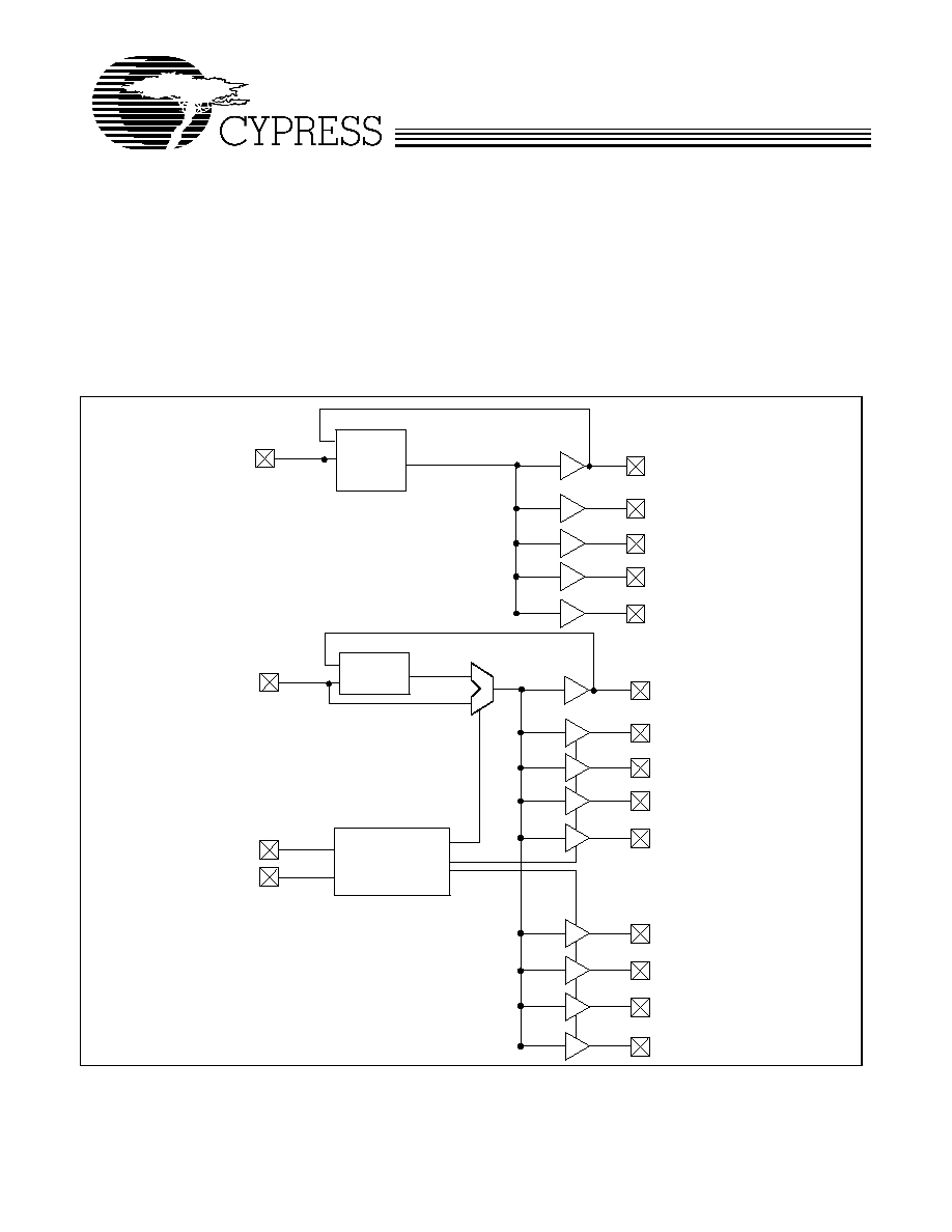
PLL
REF
CLKA1
Select Input
Decoding
S2
S1
CLKA2
CLKA3
CLKA4
CLKB1
CLKB2
CLKB3
CLKB4
CLKOUT
PLL
REF
CLK1
CLK2
CLK3
CLK4
CLKOUT
Block Diagram (Z9305)
Block Diagram (Z9309)
Z9305/Z9309
Document #: 38-07196 Rev. *A
Page 2 of 7
Product Description
The Z9309 is a low cost 3.3V zero delay buffer designed to
distribute high speed clocks in PC system devices and
SDRAM modules and is available in a 16-pin SOIC or TSSOP
package. The Z9305 is an 8-pin version of the Z9309 and it
accepts one reference input and drives out five low skew
clocks. The devices have an on-chip PLL which locks to an
input clock on the REF pin. The PLL feedback is on-chip and
is obtained from the CLKOUT pad.
The Z9309 has two banks of four outputs each, which can be
controlled by the Select inputs as shown in the Table 1. If all
output clocks are not required, Bank B can be tri-stated. The
select inputs also allow the input clock to be directly applied to
the output for chip and system testing purposes.
The Z9305 and Z9309 PLLs enter a Power Down mode when
there are no rising edges on the REF input. In this state, the
outputs are tri-stated and the PLL is turned off, resulting in less
than 50 uA of current draw. The Z9309 PLL shuts down in one
additional case as shown in Table 1.
Multiple Z9305 and Z9309 devices can accept the same input
clock and distribute it. In this case, the skew between the
outputs of two devices is guaranteed to be less than 700 ps.
All outputs have less than 200 ps of cycle-cycle jitter. The input
to output propagation delay is guaranteed to be less than 350
ps, and the output to output skew is guaranteed to be less than
250 ps.
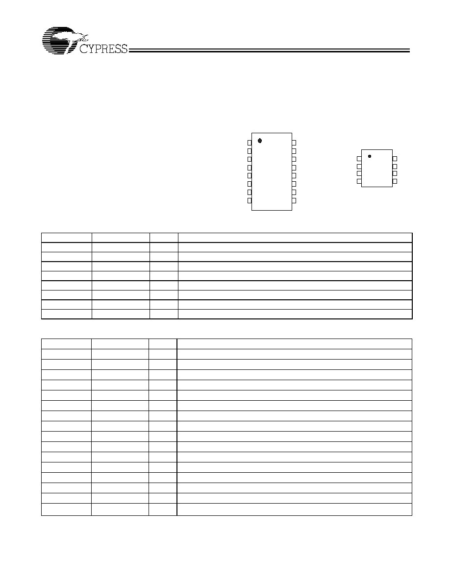
Connection Diagram
CLKOU
CLK4
VDD
CLK3
1
2
3
4
8
7
6
5
REF
CLK2
CLK1
GND
Z
9305
CLKOUT
CLKA4
CLKA3
VDD
GND
CLKB4
CLKB3
S1
1
2
3
4
5
6
7
8
16
15
14
13
12
11
10
9
REF
LKA1
LKA2
VDD
GND
LKB1
LKB2
S2
Z
9309
Pin Description (Z9305)
PIN No.
Pin Name
I/O
Description
1
REF
[1]
I
Input reference frequency, 5.0 V tolerant input
2
CLK2
[1]
O
Buffered clock output
3
CLK1
[1]
O
Buffered clock output
4
GND
I
Ground
5
CLK3
[1]
O
Buffered clock output
6
V
DD
3.3V supply
7
CLK4
[1]
O
Buffered clock output
8
CLKOUT
[1]
O
Buffered clock output, internal feedback on this pin
Pin Description (9309)
PIN No.
Pin Name
I/O
Description
1
REF
[1]
I
Input reference frequency, 5.0 V tolerant input
2
CLKA1
[1]
O
Clock output, bank A
3
CLKA2
[1]
O
Clock output, bank A
4
V
DD
I
3.3V supply
5
GND
I
Ground
6
CLKB1
[1]
O
Clock output, bank B
7
CLKB2
[1]
O
Clock output, bank B
8
S2
[2]
I
Select input pin, bit 2
9
S1
[2]
I
Select input pin, bit 1
10
CLKB3
[1]
O
Clock output, bank B
11
CLKB4
[1]
O
Clock output, bank B
12
GND
Ground
13
V
DD
3.3V supply
14
CLKA3
[1]
O
Clock output, bank A
15
CLKA4
[1]
O
Clock output, bank A
16
CLKOUT
[1]
O
Buffered output, internal feedback on this pin.
Notes:
1.
Includes weak pull-down.
2.
Includes weak pull-up.
Z9305/Z9309
Document #: 38-07196 Rev. *A
Page 3 of 7
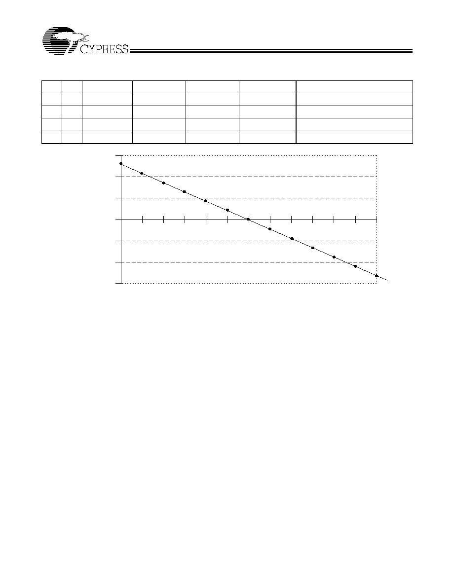
Zero Delay and Skew Control
All outputs should be uniformly loaded to achieve sero delay
between input and output. Since the CLKOUT pin is the
internal feedback to the PLL, its relative loading can adjust the
input-output delay. This is shown in the above graph.
For applications requiring zero I/O delay, all outputs including
CLKOUT must be equally loaded. Even if CLKOUT is not
used, it must have a load capacity equal to that of other
outputs. If input-to-output delay adjustments are required, use
the above graph to calculate loading differences between the
CLKOUT pin and other outputs. For zero output-output skew,
be sure to load all outputs equally.
Z9309 Select Input Functionality
S2
S1
CLKA1-A4 CLKB1-B4 CLK-OUT
[3]
Output Source
PLL Shut-down
0
0
3-state
3-state
Driven
PLL
N
0
1
Driven
3-state
Driven
PLL
N
1
0
Driven
Driven
Driven
REF
Y
1
1
Driven
Driven
Driven
PLL
N
0
-5
-10
-15
-20
-25
-30
5
10
15
20
25
30
1500
1000
500
0
-500
-1000
-1500
Ref
- I
nput
t
o
CLK
A
/
CLK
B
Delay (ps)
Output Load Difference: CLKOUT Load - CLKA/CLKB Load (PF)
REF, Input T0 CLKA/CLKB Delay versus Loading Difference Between CLKOUT and CLKA/CLKB Pins
Note:
3.
This output is driven and has an internal feedback for the PLL. The load on this output can be adjusted to change the skew between the reference and outputs.
Z9305/Z9309
Document #: 38-07196 Rev. *A
Page 4 of 7
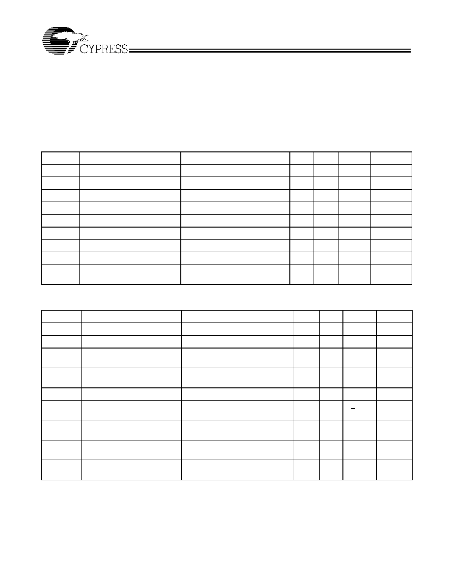
Maximum Ratings
[4]
Voltage Relative to V
SS
.................................................≠0.3V
Voltage Relative to V
DD
..................................................0.3V
Storage Temperature ................................. ≠65
∞
C to + 150
∞
C
Operating Temperature ................................. ≠40
∞
C to +85
∞
C
Maximum Power Supply ....................................................7V
Reference Input Voltage ........................................≠0.5 to 7V
This device contains circuitry to protect input against damage
from high static voltages or electric fields. Precautions should
be taken, however, to avoid applications to this circuit of any
voltage higher than the maximum rated voltages. For proper
operation, V
IN
and V
OUT
should be constrained to the range:
V
SS
< (V
IN
or V
OUT
) < V
DD
.
Unused inputs must always be tied to an appropriate logic
voltage level (either V
SS
or V
DD
).
DC Electrical Characteristics (Z9305/Z9309)
(V
DD
= 3.0 ≠ 3.6V, T
A
= ≠40
∞
C to 85
∞
C)
Parameter
Description
Test Conditions
Min.
Typ.
Max.
Units
V
IL
Input LOW Voltage4
≠
≠
0.8
Vdc
V
IH
Input HIGH Voltage4
≠
2.0
≠
Vdc
I
IL
Input LOW Current
V
IN
= 0V
50.0
µA
I
IH
Input HIGH Current
V
IN
= V
DD
±
100
µA
V
OL
Output LOW Voltage5
I
OL
= 8 mA
0.4
V
V
OH
Output HIGH Voltage5
I
OH
= ≠8mA 2.4
V
Ioz
3-state Leakage Current
S1 = S2 = GND
≠
≠
10
µA
Idd
Power-Down Supply Current
Ref = 0 MHz
≠
≠
50
µA
Idd
Dynamic Supply Current
Unload outputs, 66.66 MHz, select
inputs at V
DD
or GND.
≠
≠
40
mA
Switching Characteristics (Z9305/Z9309)
(V
DD
= 3.0 ≠ 3.6V, T
A
= ≠40
∞
C to 85
∞
C)
Parameter
Description
Test Conditions
Min.
Typ.
Max.
Units
Fin
Frequency
30 pF load
10
150
MHz
≠
Duty Cycle (T
2
/T
1
)
[7]
Measured @ 1.4V
45
50
55
%
t
3
Rise Time
[7]
Measured between 0.8V and 2.0V
15 pF Load
≠
1.5
nSec
t
4
Fall Time
[7]
Measured between 0.8V and 2.0V
15 pF Load
1.5
nSec
t
5
Output-to-Output Skew
[7]
All output equally loaded
≠
≠
250
pSec
t
6
Delay, REF Rising Edge to
CLKOUT Rising Edge
[7]
Measured at V
DD
/2
≠
0
+ 350
pSec
t
7
Device-to-Device Skew
[7]
Measured at V
DD
/2 on FBK pins of
devices
-
0
700
pSec
tj
Cycle-to-Cycle Jitter
[7]
Measured at 66.67 MHz, loaded
outputs, input Trise/Fall < 1 nS
≠
≠
200
pSec
tLOCK
Maximum PLL Lock Time
[7]
Stable power supply, valid clocks
presented on REF pin.
1.0
ms
Notes:
4.
Multiple Supplies: The voltage on any input or I/O pin cannot exceed the power pin during power-up. Power supply sequencing is NOT required.
5.
REF and FBK inputs have a threshold voltage of V
DD
/2.
6.
Parameter is guaranteed by design and characterization. Not 100% tested in production. All parameters specified with loaded outputs.
7.
Parameter is guaranteed by design and characterization. Not 100% tested in production. All parameters specified with loaded outputs.
Z9305/Z9309
Document #: 38-07196 Rev. *A
Page 5 of 7
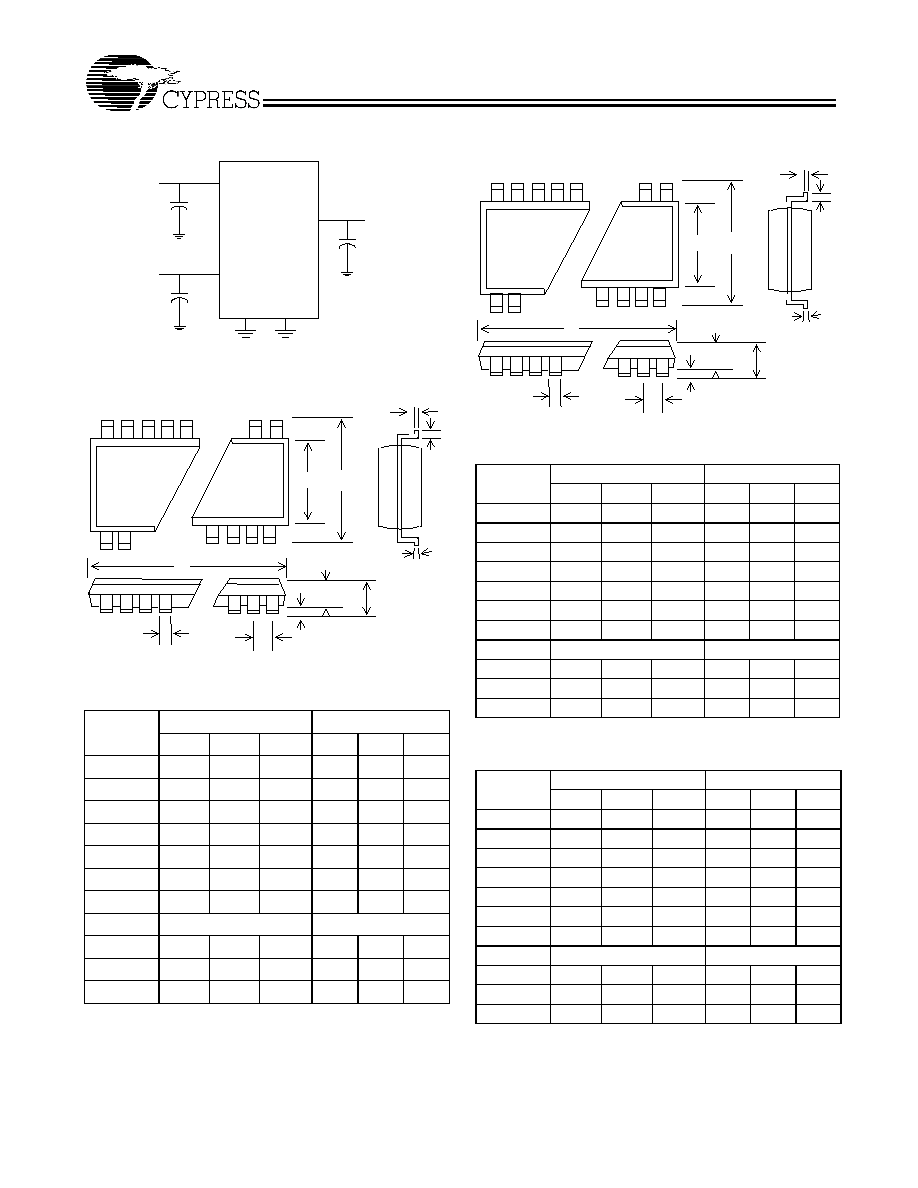
Test Circuit Diagram
Package Drawing and Dimensions
Package Drawing and Dimensions (16-pin
150-mil SOIC)
8-pin SOIC Outline Dimensions
Parameter
Inches
Millimeters
Min.
Nom.
Max.
Min.
Nom.
Max.
A
0.053
-
0.069
1.35
-
1.75
A
1
0.004
-
0.010
0.10
-
0.25
A2
0.047
-
0.059
1.20
-
1.50
B
0.013
-
0.020
0.33
-
0.51
C
0.007
-
0.010
0.19
-
0.25
D
0.189
-
0.197
4.80
-
5.00
E
0.150
-
0.157
3.80
-
4.00
e
0.050 BSC
1.27 BSC
H
0.228
-
0.244
5.80
-
6.20
L
0.016
-
0.050
0.40
-
1.27
a
0∫
-
8∫
0∫
-
8∫
VDD
VDD
GND
GND
Outputs
0.1 uF
0.1 uF
CLK out
C
LOAD
Test Circuit
a
B
e
A
A
1
A
2
D
E
H
L
C
16-pin SOIC Outline Dimensions (150 mil)
Parameter
Inches
Millimeters
Min.
Nom.
Max.
Min.
Nom.
Max.
A
0.053
-
0.069
1.35
-
1.75
A
1
0.004
-
0.010
0.10
-
0.25
A2
0.047
-
0.059
1.20
-
1.50
B
0.013
-
0.020
0.33
-
0.51
C
0.007
-
0.010
0.19
-
0.25
D
0.366
-
0.394
9.80
-
10.00
E
0.150
-
0.157
3.80
-
4.00
e
0.050 BSC
1.27 BSC
H
0.228
-
0.244
5.80
-
6.20
L
0.016
-
0.050
0.40
-
1.27
a
0∫
-
8∫
0∫
-
8∫
16-pin TSSOP Outline Dimensions
Parameter
Inches
Millimeters
Min.
Nom.
Max.
Min.
Nom.
Max.
A
-
-
0.047
-
-
1.20
A
1
0.002
-
0.006
0.05
-
0.15
A2
0.031
0.039
0.041
0.80
1.00
1.05
B
0.007
-
0.012
0.19
-
0.30
C
0.004
-
0.008
0.09
-
0.20
D
0.193
0.197
0.201
4.90
5.00
5.10
E
0.169
0.173
0.177
4.30
4.40
4.50
e
0.026 BSC
0.65 BSC
H
0.244
0.252
0.260
6.20
6.40
6.60
L
0.018
0.024
0.030
0.45
0.60
0.75
a
0∫
-
8∫
0∫
-
8∫
a
B
e
A
A
1
A
2
D
E
H
L
C