 | –≠–ª–µ–∫—Ç—Ä–æ–Ω–Ω—ã–π –∫–æ–º–ø–æ–Ω–µ–Ω—Ç: LM317L3 | –°–∫–∞—á–∞—Ç—å:  PDF PDF  ZIP ZIP |
CYStech Electronics Corp.
Spec. No. : C513L3
Issued Date : 2003.04.09
Revised Date :2005.05.03
Page No. : 1/9
LM317L3
CYStek Product Specification
Three Terminal Adjustable Output
Positive Voltage Regulators
LM317L3
The LM317L3 is an adjustable 3≠terminal positive voltage regulator capable of supplying in excess of
1.5A over an output voltage range of 1.2 V to 37 V. This voltage regulator is exceptionally easy to use and
requires only two external resistors to set the output voltage. Further, it employs internal current limiting,
thermal shutdown and safe area compensation, making it essentially blow≠out proof.
The LM317L3 serves a wide variety of applications including local, on-card regulation. This device can
also be used to make a programmable output regulator, or by connecting a fixed resistor between the
adjustment and output, the LM317L3 can be used as a precision current regulator.
Output Current in Excess of 1.5 A
Output Adjustable between 1.2 V and 37 V
Internal Thermal Overload Protection
Internal Short Circuit Current Limiting Constant with Temperature
Output Transistor Safe≠Area Compensation
Floating Operation for High Voltage Applications
Eliminates Stocking many Fixed Voltages
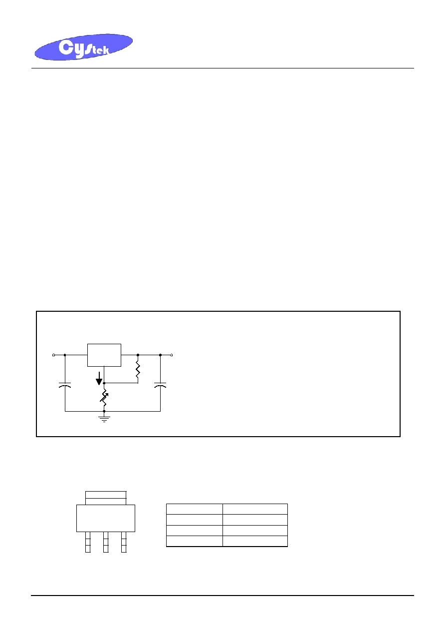
Standard Application
+
+
PL317
R1
R2
Cout
Cin
Vin
Vout
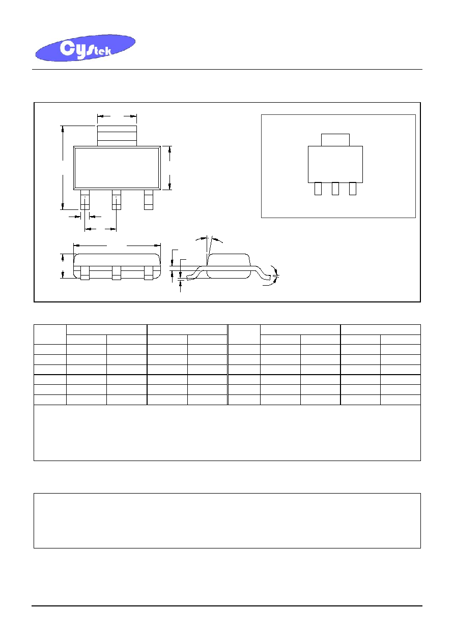
Package Information
SOT-223
Pin Function
1 ADJ
2 OUTPUT
3 INPUT
1.0µF
0.1µF
Cin is required if regulator is located an appreciate
distance from power supply filter.
Cout is not needed for stability, however, it does
improve transient response.
V
out=
1.25(
1+
R
2/
R
1
)+I
Adj
R
2
Since
I
Adj
is controlled to less than 100 µA, the
error associated with this term is negligible in
most applications.
I
Adj
1 2 3
LM317
CYStech Electronics Corp.
Spec. No. : C513L3
Issued Date : 2003.04.09
Revised Date :2005.05.03
Page No. : 2/9
LM317L3
CYStek Product Specification
Maximum Ratings
Rating Symbol
Value
Unit
Input-Output Voltage Differential
V
I
-V
O
40 V
Power Dissipation
T
A
=25
P
D
Internally
Limited W
Operating Junction Temperature Range
T
J
-40 to +125
Storage Temperature Range
Tstg
-65 to +150
Electrical Characteristics
(V
I
-V
O
=5V,I
O
=0.5A,T
J
=0 to 125, unless otherwise noted
)
Characteristics
Symbol
Conditions
Min Typ Max Unit
Line Regulation(
Note 1
)
Reg
line
T
A
=25,3.0VV
I
-V
O
40V
- 0.01
0.04 %/V
Load Regulation(
Note 1
) Reg
load
T
A
=25,10mAI
O
1.5A
V
O
5.0V
V
O
5.0V
-
-
5.0
0.1
25
0.5
mV
%V
O
Thermal Regulation(
Note 4
)
Reg
therm
T
A
=25, 20ms pulse
- 0.03
0.07
%V
O
/W
Adjust Pin Current
I
Adj
- 50 100 µA
Adjust Pin Current Change I
Adj
2.5VV
I
-V
O
40V,10mAI
L
1.5A
P
D
5W
- 0.2 5.0 µA
Reference Voltage
Vref
3.0VV
I
-V
O
40V,10mAI
O
1.5A
P
D
5W
1.2 1.25 1.3 V
Temperature Stability
Ts
0
T
J
125
- 0.7 - %V
O
Minimum Load Current to
maintain Regulation
I
Lmin
V
I
-V
O
=40V -
3.5
10
mA
Maximum Output Current Imax
V
I
-V
O
15V,P
D
5W
V
I
-V
O
40V,P
D
5W,T
A
=25
1. 5
0.15
2.2
0.4
-
-
A
RMS Noise
N
% of V
O
,T
A
=25,10Hzf10kHz
- 0.003 - %V
O
Ripple Rejection(
Note 2
) RR V
O
=10V,f=120Hz
Without C
Adj
C
Adj
=10µF
-
66
65
80
-
-
dB
Long-Term Stability(
Note 3)
S
T
J
=125,T
A
=25 for endpoint
measurements
- 0.3 1.0
%/1.0k
Hrs
Notes:
1.Load and line regulation are specified at constant junction temperature. Changes in V
O
due to heating effects must be
taken into account separately. Pulse testing with low duty cycle is used.
2.C
Adj
, when used, is connected between the adjustment pin and ground.
3.Since long-term stability cannot be measured on each device before shipment, this specification is an engineering
estimate of average stability from lot to lot.
4.Power dissipation within an IC voltage regulator produces a temperature gradient on the die, affecting individual IC
components on the die. These effects can be minimized by proper integrated circuit design and layout techniques.
Thermal regulation is the effect of these temperature gradients on the output voltage and is expressed in percentage
of output change per watt of power change in a specified time.
CYStech Electronics Corp.
Spec. No. : C513L3
Issued Date : 2003.04.09
Revised Date :2005.05.03
Page No. : 3/9
LM317L3
CYStek Product Specification
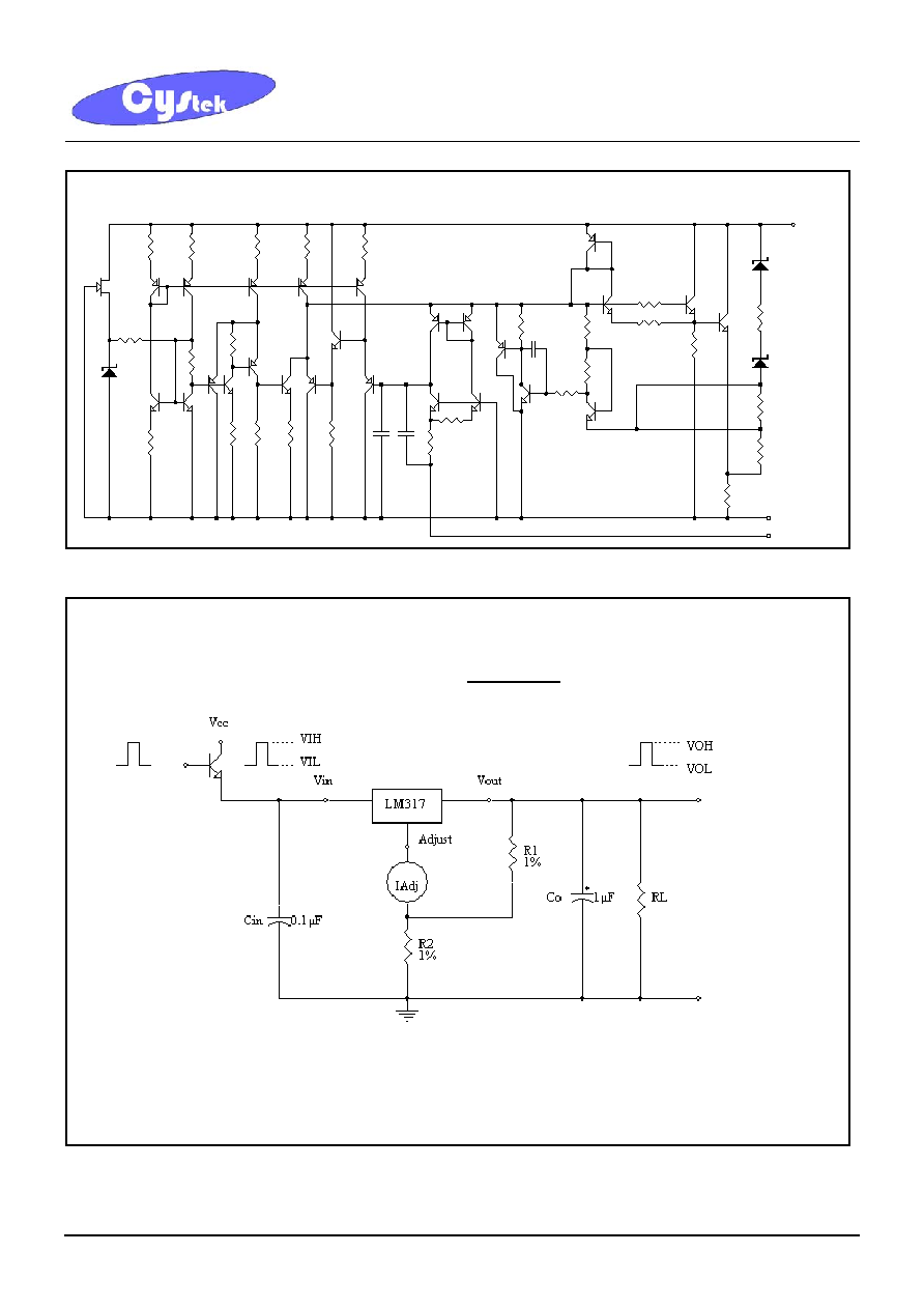
Representative Schematic Diagram
Vin
Vout
Adjust
Fig 1. Line Regulation and I
Adj
/Line test circuit
Pulse testing required
1% Duty Cycle is
suggested
V
OH
-V
OL
Line Regulation(%/V)= ◊100
V
OL
CYStech Electronics Corp.
Spec. No. : C513L3
Issued Date : 2003.04.09
Revised Date :2005.05.03
Page No. : 4/9
LM317L3
CYStek Product Specification
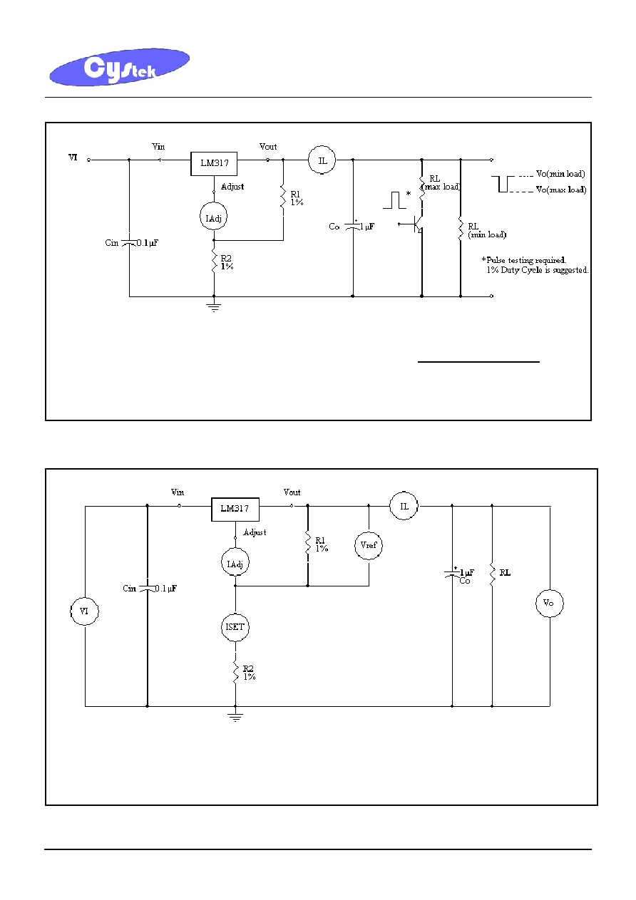
Vo(min load)-Vo(max load)
Load Regulation(mV)=Vo(min load)-Vo(max load) Load Regulation(%Vo)= ◊100
Vo(min load)
Fig 2. Load Regulation and I
Adj
/Load test circuit
Pulse testing required.
1% Duty Cycle is suggested.
To calculate R2: Vout=I
SET
R2+1.250V
Assume I
SET
=5.25mA
Fig 3. Standard Test Circuit
CYStech Electronics Corp.
Spec. No. : C513L3
Issued Date : 2003.04.09
Revised Date :2005.05.03
Page No. : 5/9
LM317L3
CYStek Product Specification
Application Information
Basic Circuit Operation
The LM317 is a 3-terminal floating regulator. In operation, the LM317 develops and maintains a nominal
1.25V reference (Vref) between its output and adjustment terminals. This reference voltage is converted
to a programming current (Iprog) by R
1
(see Fig 5), and this constant current flows through R
2
to ground.
The regulated output voltage is given by:
Vout=Vref
(
1+R
2
/R
1
)+I
Adj
R
2
Since the current from the adjustment terminal (I
Adj
) represents an error term in the equation, the LM317
was designed to control I
Adj
to less than 100 µA and keep it constant. To do this, all quiescent operating
current is returned to the output terminal. This imposes the requirement for a minimum load current. If
the load current is less than this minimum, the output voltage will rise.
Since the LM317 is a floating regulator, it is only the voltage differential across the circuit which is
important to performance, and operation at high voltages with respect to ground is possible.
Fig 4. Ripple Rejection Test Circuit
Fig 5. Basic Circuit Configuration
CYStech Electronics Corp.
Spec. No. : C513L3
Issued Date : 2003.04.09
Revised Date :2005.05.03
Page No. : 6/9
LM317L3
CYStek Product Specification
Load Regulation
The LM317 is capable of providing extremely good load regulation, but a few precautions are needed to
obtain maximum performance. For best performance, the programming resistor (R
1
) should be connected
as close to the regulator as possible to minimize line drops which effectively appear in series with the
reference, thereby degrading regulation. The ground end of R
2
can be returned near the load ground to
provide remote ground sensing and improve load regulation.
External Capacitors
A 0.1µF disc or 1.0µF tantalum input bypass capacitor (Cin) is recommended to reduce the sensitivity to
input line impedance.
The adjustment terminal may be bypassed to ground to improve ripple rejection. This capacitor (C
Adj
)
prevents ripple from being amplified as the output voltage is increased. A 10µF capacitor should improve
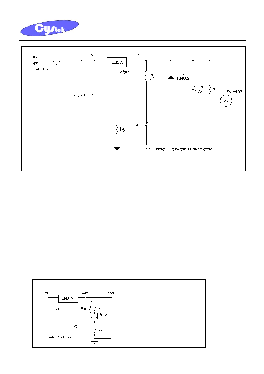
ripple rejection about 15 dB at 120 Hz in a 10V application.
Although the LM317 is stable with no output capacitance, like any feedback circuit, certain values of
external capacitance can cause excessive ringing. An output capacitance (Co) in the form of a 1.0µF
tantalum or 25µF aluminum electrolytic capacitor on the output swamps this effect and insures stability.
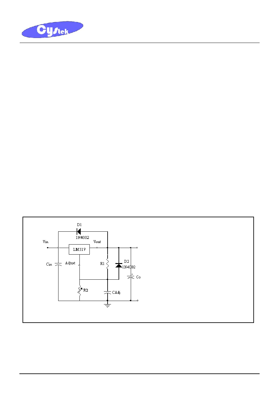
Protection Diodes
When external capacitors are used with any IC regulator, it is sometimes necessary to add protection
diodes to prevent the capacitors from discharging through low current points into the regulator.
Fig 6 shows the LM317 with the recommended protection diodes for output voltages in excess of 25V or
high capacitance values (Co>25µF,C
Adj
>10µF). Diode D
1
prevents Co from discharging thru the IC
during an input short circuit. Diode D
2
protects against capacitor C
Adj
discharging through the IC during
an output short circuit. The combination of diodes D
1
and D
2
prevents C
Adj
from discharging through the
IC during an input short circuit.
Fig 6. Voltage Regulator with Protection Diodes
CYStech Electronics Corp.
Spec. No. : C513L3
Issued Date : 2003.04.09
Revised Date :2005.05.03
Page No. : 7/9
LM317L3
CYStek Product Specification
Application Circuits
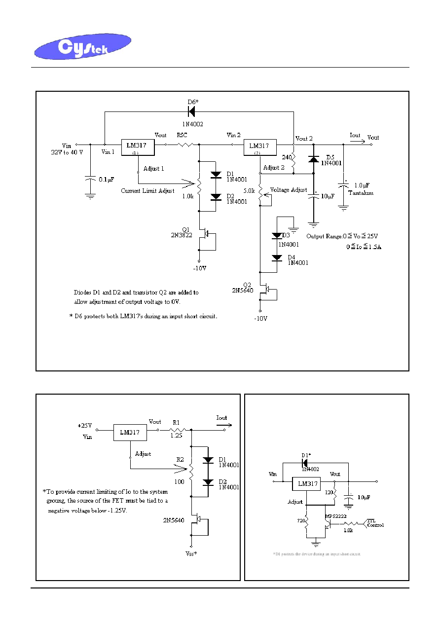
Fig 7. "Laboratory" Power Supply with Adjustable Current Limit and Output Voltage
R1=Vref/(Iomax+I
DSS
) R2Vref/I
DSS
Vo
<
BV
DSS
+1.25V+Vss
I
Lmin
-I
DSS
<Io<1.5A
As shown 0<Io<1.0A
Fig 8. Adjustable Current Limiter
Fig 9. 5.0V Electronic Shutdown Regulator
CYStech Electronics Corp.
Spec. No. : C513L3
Issued Date : 2003.04.09
Revised Date :2005.05.03
Page No. : 8/9
LM317L3
CYStek Product Specification
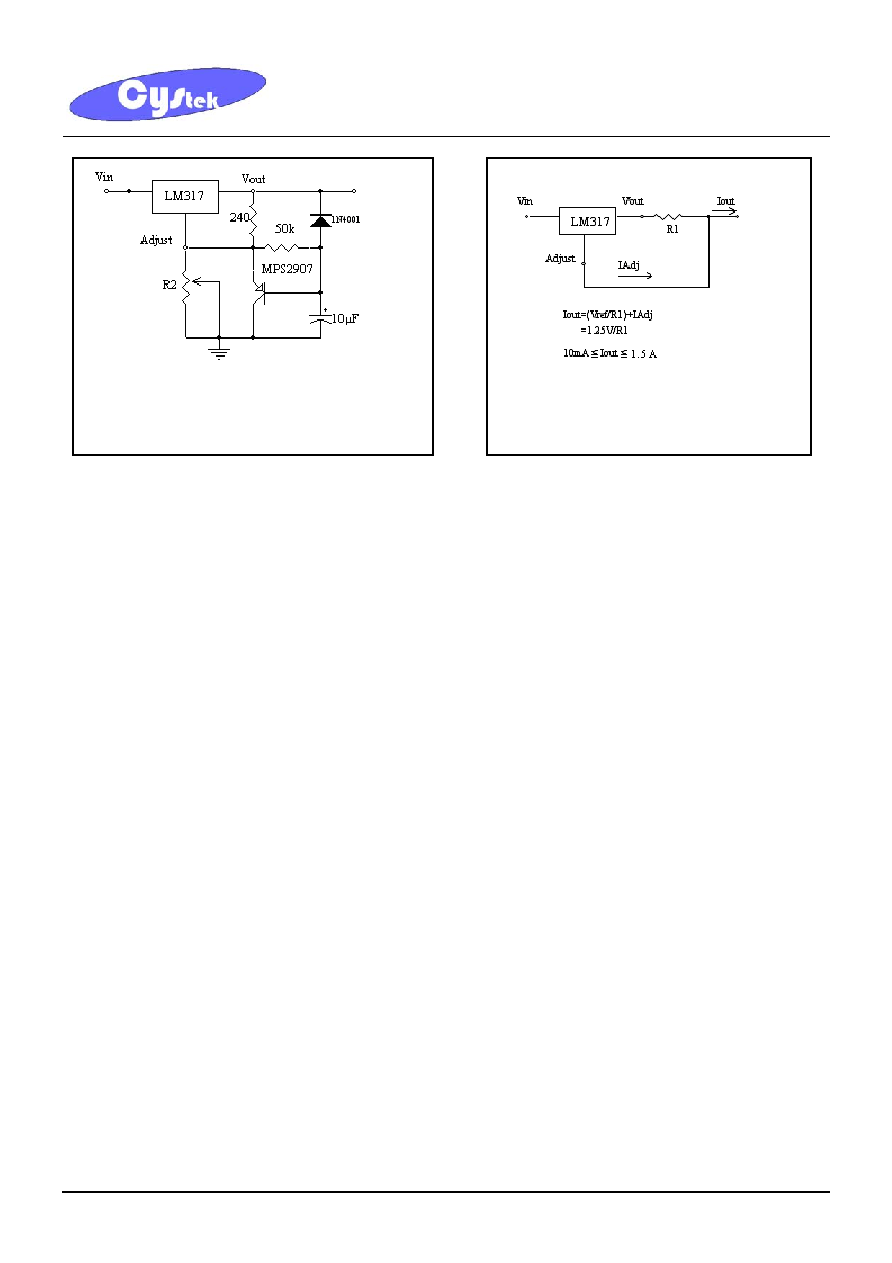
Fig 10. Slow Turn-on Regulator
Fig 11. Current Regulator
CYStech Electronics Corp.
Spec. No. : C513L3
Issued Date : 2003.04.09
Revised Date :2005.05.03
Page No. : 9/9
LM317L3
CYStek Product Specification
SOT-223 Dimension
*: Typical
Inches Millimeters
Inches Millimeters
DIM
Min. Max. Min. Max.
DIM
Min. Max. Min. Max.
A 0.1142
0.1220 2.90 3.10 G 0.0551
0.0709 1.40 1.80
B 0.2638
0.2874 6.70 7.30 H 0.0098
0.0138 0.25 0.35
C 0.1299
0.1457 3.30 3.70 I 0.0008
0.0039 0.02 0.10
D 0.0236
0.0315 0.60 0.80 a1 *13
o
- *13
o
-
E *0.0906 -
*2.30
-
a2 0
o
10
o
0
o
10
o
F
0.2480
0.2638
6.30
6.70
Notes:
1.Controlling dimension: millimeters.
2.Maximum lead thickness includes lead finish thickness, and minimum lead thickness is the minimum thickness of base material.
3.If there is any question with packing specification or packing method, please contact your local CYStek sales office.
Material:
∑
Lead: 42 Alloy; solder plating
∑
Mold Compound: Epoxy resin family, flammability solid burning class: UL94V-0
Important Notice:
∑
All rights are reserved. Reproduction in whole or in part is prohibited without the prior written approval of CYStek.
∑
CYStek reserves the right to make changes to its products without notice.
∑
CYStek semiconductor products are not warranted to be suitable for use in Life-Support Applications, or systems.
∑
CYStek assumes no liability for any consequence of customer product design, infringement of patents, or application assistance.
3
2
1
F
B
A
C
D
E
G
H
a1
a2
I
Style: Pin 1.Adj 2.Output 3.Input
Marking:
3-Lead SOT-223 Plastic
Surface Mounted Package
CYStek Package Code: L3
317