LUPA-1300
Datasheet
Cypress Semiconductor Corporation
3901 North First Street
San Jose, CA 95134
408-943-2600
Contact info@Fillfactory.com Document # : 38-05711 Rev.**( Revision 3.1) Page 3 of 48
T
able of contents
1
PREAMBLE .................................................................................................................................5
1.1
O
VERVIEW
..............................................................................................................................5
1.2
M
AIN FEATURES
......................................................................................................................5
1.3
P
ART
N
UMBER
........................................................................................................................6
2
SPECIFICATIONS ......................................................................................................................7
2.1
G
ENERAL SPECIFICATIONS
.......................................................................................................7
2.2
E
LECTRO
-
OPTICAL CHARACTERISTICS
.....................................................................................7
2.2.1
Overview.........................................................................................................................7
2.2.2
Features and general specifications..............................................................................8
2.2.3
Spectral response curve .................................................................................................9
2.2.4
Photo-voltaic response curve.......................................................................................10
2.3
E
LECTRICAL SPECIFICATIONS
................................................................................................11
2.3.1
Absolute maximum ratings..........................................................................................11
2.3.2
Recommended operating conditions ...........................................................................11
3
SENSOR ARCHITECTURE ....................................................................................................13
3.1
P
IXEL ARCHITECTURE
............................................................................................................14
3.2
C
OLUMN READOUT AMPLIFIERS
.............................................................................................15
3.3
O
UTPUT AMPLIFIERS
..............................................................................................................16
3.4
F
RAME RATE AND WINDOWING
..............................................................................................17
3.4.1
Frame rate calculation ................................................................................................17
3.4.2
X-Y addressing and windowing...................................................................................17
3.5
T
EMPERATURE REFERENCE CIRCUITS
....................................................................................18
3.5.1
Temperature diode.......................................................................................................18
3.5.2
Temperature module....................................................................................................18
3.6
S
YNCHRONOUS SHUTTER
.......................................................................................................20
3.7
N
ON
-
DESTRUCTIVE READOUT
(NDR)....................................................................................21
3.8
O
PERATION AND SIGNALING
..................................................................................................21
3.8.1
Power supplies and grounds........................................................................................22
3.8.2
Biasing and analog signals .........................................................................................24
3.8.3
Pixel array signals .......................................................................................................24
3.8.4
Digital signals ..............................................................................................................26
3.8.5
Test signals...................................................................................................................27
4
TIMING ......................................................................................................................................28
4.1
T
IMING OF THE PIXEL ARRAY
.................................................................................................28
4.2
R
EADOUT OF THE PIXEL ARRAY
.............................................................................................29
4.2.1
Reduced Row Overhead Time timing..........................................................................31
4.3
T
IMING OF THE
S
ERIAL
P
ARALLEL
I
NTERFACE
(SPI).............................................................33
5
PIN CONFIGURATION ...........................................................................................................34
6
PAD POSITIONING AND PACKAGING ..............................................................................39
6.1
P
ACKAGE
...............................................................................................................................39
6.2
P
ACKAGE AND DIE
.................................................................................................................40
6.3
C
OLOR FILTER
.......................................................................................................................41
6.4
G
LASS TRANSMITTANCE
........................................................................................................42
6.4.1
Monochrome................................................................................................................42
6.4.2
Color.............................................................................................................................42
6.5
H
ANDLING AND
S
TORAGE PRECAUTIONS
...............................................................................43

LUPA-1300
Datasheet
Cypress Semiconductor Corporation
3901 North First Street
San Jose, CA 95134
408-943-2600
Contact info@Fillfactory.com Document # : 38-05711 Rev.**( Revision 3.1) Page 5 of 48
1 Preamble
1.1 Overview
This document describes the interfacing and the driving of the image sensor
LUPA1300, which is a 1280 by 1024 CMOS pixel array working at 450 frames/sec.
The sensor is an active pixel sensor with synchronous shutter. The pixel size is 14 *
14 µm and the sensor is designed to achieve a fame rate of 450 frames/sec at full
resolution. This high frame rate can be achieved by 16 parallel output amplifiers each
working at 40MHz pixel rate.
The readout speed can be boosted by means of windowed Region Of Interest (ROI)
readout. High dynamic range scenes can be captured using the double slope
functionality.
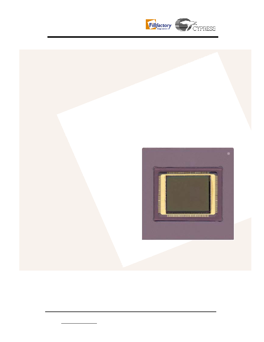
The sensor uses a 3-wire Serial-Parallel (SPI) interface. It is housed in a 145-pin
ceramic PGA package.
In the following sections the different modules of the image sensor are discussed
more into detail. This datasheet allows the user to develop a camera-system based on
the described timing and interfacing.
1.2 Main
features
The main features of the image sensor are identified as:
· SXGA resolution: 1280 x 1024 active pixels.
· 14
µ
m
2
square pixels (based on the high-fill factor active pixel sensor
technology of FillFactory (US patent No. 6,225,670 and others)).
· Pixel rate of 40 MHz using 16 parallel outputs.
· Random programmable windowing.
· Dual slope integration possible
· 145-pin PGA package
· Peak QE x FF of 15%.
· Optical format: 1,43" (17.9 mm x 14.3 mm)
· Optical dynamic range: 62 dB (1330:1) in single slope operation and 80...100
dB in double slope operation.
· 16 parallel analog output amplifiers.
· Synchronous pipelined shutter.
· Processing is done in a CMOS 0.50 µm triple metal process.