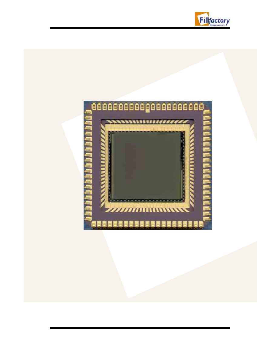
Star1000
1 Mega pixel rad-hard CMOS APS
7/16/2003
Page 2 of 20
Table of contents
1.
SENSOR DESCRIPTION ............................................................................................................................... 3
1.1.
The pixel array........................................................................................................................................ 4
1.2.
Addressing logic..................................................................................................................................... 4
1.3.
The column amplifiers ........................................................................................................................... 5
1.4.
The output amplifier and analog multiplexer ........................................................................................ 5
1.5.
The ADC................................................................................................................................................. 5
2.
IMAGE SENSOR SPECIFICATIONS ........................................................................................................... 6
2.1.
General specifications ............................................................................................................................ 6
2.2.
Electro-optical specifications................................................................................................................. 6
2.3.
Spectral response curve.......................................................................................................................... 8
2.4.
Photo-voltaic response ........................................................................................................................... 8
2.5.
Absolute maximum ratings .................................................................................................................... 9
2.6.
DC operating conditions......................................................................................................................... 9
3.
TIMING AND CONTROL SIGNALS ......................................................................................................... 10
3.1.
Row selection and reset timing ............................................................................................................ 10
3.2.
Pixel read-out timing............................................................................................................................ 12
4.
PIN LIST ........................................................................................................................................................ 13
5.
PACKAGING AND GEOMETRICAL CONSTRAINTS ........................................................................... 17
5.1.
Package drawing................................................................................................................................... 17
5.2.
Die alignment ....................................................................................................................................... 18
APPENDIX A:
STAR1000 EVALUATION SYSTEM................................................................................. 19
APPENDIX B:
FREQUENTLY ASKED QUESTIONS ............................................................................... 20
Document history record
Issue
Date
Description of changes
6.1 4
th
April, 2003
p6: Table 1: image sensor specs updated.
p8: Spectral response curve and photovoltaic
response curve added.
p18: Package drawing added.
p19: Appendix A added.
p20: Appendix B added.
6.2 23
rd
April, 2003
p6: Table 1: image sensor specs updated.
p8: Photovoltaic response curve updated.
p17: Table 9: VDD_ANA connected
internally...
6.3 8
th
July, 2003
p6: Table 2: values updated.
p9: Table 3 and 4 added.
p13: Pin connection drawing added.
p14: Table 7 updated.
p16: Notes added.
p17: Package drawing updated.
p18: Die alignment added.
Star1000
1 Mega pixel rad-hard CMOS APS
7/16/2003
Page 3 of 20
1. Sensor description
The STAR1000 is a CMOS image sensor with 1024 by 1024 pixels on a 15-
µm pitch.
It features on-chip Fixed Pattern Noise (FPN) correction, a programmable gain
amplifier and a 10-bit Analog to Digital Converter (ADC).
All circuits are designed using the radiation tolerant design rules for CMOS image
sensors to allow a high tolerance against total dose effects.
Registers that can be directly accessed by the external controller contain the X- and
Y-addresses of the pixels to be read. This architecture provides flexible operation and
allows different operation modes like (multiple) windowing, sub sampling, etc.
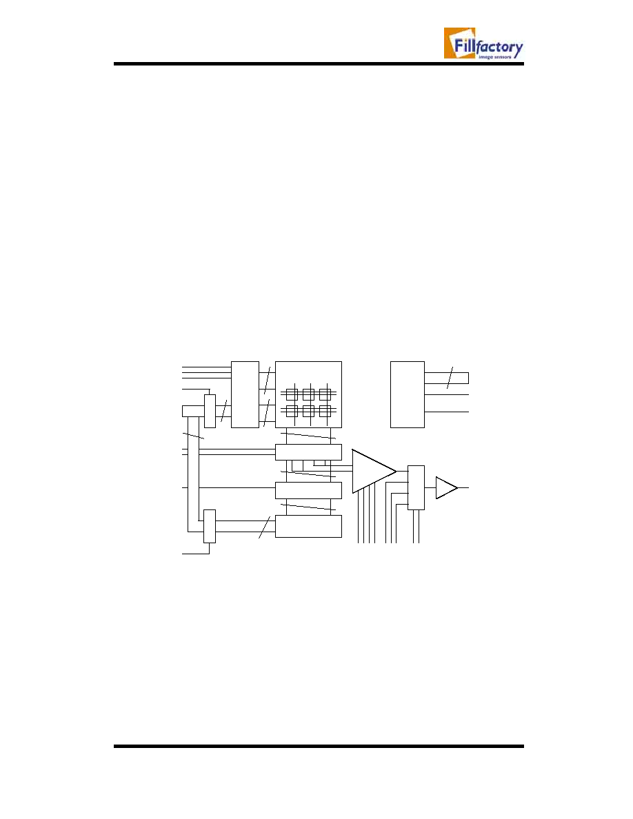
The image sensor contains five sections: the pixel array, the X-and Y addressing
logic, the column amplifiers, the output amplifier and the ADC. Figure 1 shows an
outline diagram of the sensor, including an indication of the main control signals. The
following paragraphs explain in more detail the function and operation of the different
imager parts.
Figure 1: Image sensor outline diagram
Pixel Array
1024 x 1024 pixels
Y address
decoder
and logic
Reset
Reset DS
Vref
10
A0 ... A9
Column amplifiers
S
R
X register
1024
1024
1024
Clk X
1024
X Address Decoder
10
10
Buffer
1024
La
t
c
h
La
t
c
h
Progr. gain
amplifier
M
u
l
tipl
e
xer
Bl
ackr
e
f
Ca
l
G0f G
1
Ai
n
1
Ai
n
2
Ai
n
3
Se
l
0
Se
l
1
Aout
10-bit ADC
10
D0 ... D9
Clk ADC
Ain
1024
Rst
Rd
Col
Ld Y
Ld X
Rst
Rd
1024 Rst
Sig
Star1000
1 Mega pixel rad-hard CMOS APS
7/16/2003
Page 4 of 20
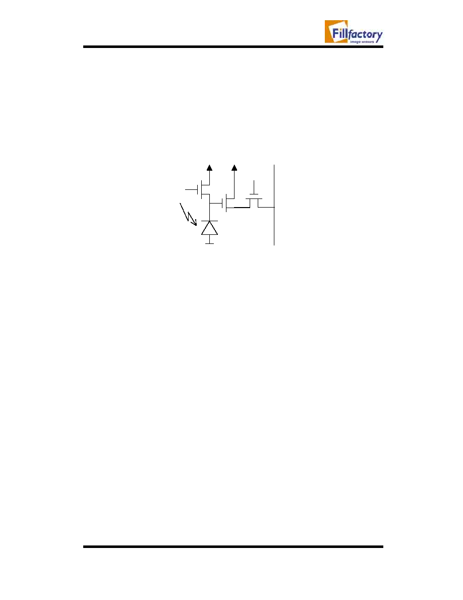
1.1. The
pixel
array
The pixel array contains 1024 by 1024 active pixels at 15
µm pitch. Each pixel
contains one photo diode and three transistors (Figure 2).
The photo diode is always in reverse bias. At the beginning of the integration cycle a
pulse is applied to the reset line (gate of T1) bringing the cathode of D1 to the reset
voltage level. During the integration period photon-generated electrons accumulate
on the diode capacitance, reducing the voltage on the gate of T2. The real
illumination-dependent signal is the different between the reset level and the output
level after integration. This difference is made in the column amplifiers. T2 acts as a
source follower and T3 allows connection of the pixel signal (reset level and output
level) to the vertical output bus.
The reset-lines and the read-lines of the pixels in a row are connected together to the
Y-decoder logic; the outputs of the pixels in a column are connected together to a
column amplifier.
1.2. Addressing
logic
The addressing logic allows direct addressing of rows and columns. Instead of the
one-hot shift registers that are often used, address decoders are implemented. One can
select a line by presenting the required address to the address input of the device and
latching it to the Y-decoder logic. Presenting the X-address to the device address
input and latching it to the X-address decoder can select a column.
A typical line read out sequence will first select a line by applying the Y-address to
the Y-decoder. Activation of the "LD_Y" input on the Y-logic will connect the pixel
outputs of the selected line to the column amplifiers. The individual column amplifier
outputs can be connected to the output amplifier by applying the respective X-
addresses to the X address decoder. Applying the appropriate Y-address to the Y-
decoder and activating the "Reset" input reset a line. The integration time of a row is
the time between the last reset of this row and time when it is selected for read-out.
The Y-decoder logic has two different reset inputs: "RESET" and "RESET_DS".
Activation of "RESET" will reset the pixel to the Vdd level; activation of
"RESET_DS" will reset the pixel to the voltage level on the "VREF" input. This
Reset
Read
C
o
lum
n
bus
T1
T2
T3
Figure 2: Active pixel electrical diagram

Star1000
1 Mega pixel rad-hard CMOS APS
7/16/2003
Page 5 of 20
feature allows the application of the so-called dual slope integration (see APPENDIX
B). If dual slope integration is not needed "VREF" can be tied to Vdd and
"RESET_DS" must never be activated.
1.3.
The column amplifiers
All outputs from the pixels in a column are connected in parallel to a column
amplifier. This amplifier samples the output voltage and the reset level of the pixel
whose row is selected at that moment and presents these voltage levels to the output
amplifier. As a result the pixels are always reset immediately after read-out as part of
the sample procedure and the maximum integration time of a pixel is the time
between two read cycles.
1.4. The
output
amplifier and analog multiplexer
The output amplifier combines subtraction of pixel signal level from reset level with a
programmable gain amplifier. Since the amplifier is AC coupled it also contains a
provision to maintain and restore the proper DC level.
An analogue signal multiplexer feeds the pixel signal to the final unity gain buffer to
provide the required drive capability. Apart from the pixel signal also three other
external analogue signals can be fed to the output buffer. All these signals can be
digitalised by the on-chip ADC if the output of this buffer is externally connected to
the input of the ADC.
The purpose of the additional analogue inputs ("A_IN1", "A_IN2" and "A_IN3") is to
allow a possibility to process other analogue signals through the image sensors signal
path. These signals can thus be converted by the ADC and processed by the image
controller FPGA. The additional analogue inputs are intended for low frequency or
DC signals and have a reduced bandwidth, compared with the image signal path.
1.5. The
ADC
The image sensor has a 10-bit ADC that is electrically separated from the rest of the
image sensor circuits and can be powered down if an external ADC is used. The
conversion takes place at the falling edge of the clock and the output pins can be
disabled to allow operation of the device in a bus structure.