Äîêóìåíòàöèÿ è îïèñàíèÿ www.docs.chipfind.ru

5V, 3.3V, ISRTM High-Performance CPLDs
Ultra37000 CPLD Family
Cypress Semiconductor Corporation
·
3901 North First Street
·
San Jose
,
CA 95134
·
408-943-2600
Document #: 38-03007 Rev. *B
Revised May 7, 2003
Features
· In-System ReprogrammableTM (ISRTM) CMOS CPLDs
-- JTAG interface for reconfigurability
-- Design changes do not cause pinout changes
-- Design changes do not cause timing changes
· High density
-- 32 to 512 macrocells
-- 32 to 264 I/O pins
-- Five dedicated inputs including four clock pins
· Simple timing model
-- No fanout delays
-- No expander delays
-- No dedicated vs. I/O pin delays
-- No additional delay through PIM
-- No penalty for using full 16 product terms
-- No delay for steering or sharing product terms
· 3.3V and 5V versions
· PCI-compatible
[1]
· Programmable bus-hold capabilities on all I/Os
· Intelligent product term allocator provides:
-- 0 to 16 product terms to any macrocell
-- Product term steering on an individual basis
-- Product term sharing among local macrocells
· Flexible clocking
-- Four synchronous clocks per device
-- Product term clocking
-- Clock polarity control per logic block
· Consistent package/pinout offering across all densities
-- Simplifies design migration
-- Same pinout for 3.3V and 5.0V devices
· Packages
-- 44 to 400 leads in PLCC, CLCC, PQFP, TQFP, CQFP,
BGA, and Fine-Pitch BGA packages
General Description
The Ultra37000TM family of CMOS CPLDs provides a range of
high-density programmable logic solutions with unparalleled
system performance. The Ultra37000 family is designed to
bring the flexibility, ease of use, and performance of the 22V10
to high-density CPLDs. The architecture is based on a number
of logic blocks that are connected by a Programmable Inter-
connect Matrix (PIM). Each logic block features its own
product term array, product term allocator, and 16 macrocells.
The PIM distributes signals from the logic block outputs and all
input pins to the logic block inputs.
All of the Ultra37000 devices are electrically erasable and In-
System Reprogrammable (ISR), which simplifies both design
and manufacturing flows, thereby reducing costs. The ISR
feature provides the ability to reconfigure the devices without
having design changes cause pinout or timing changes. The
Cypress ISR function is implemented through a JTAG-
compliant serial interface. Data is shifted in and out through
the TDI and TDO pins, respectively. Because of the superior
routability and simple timing model of the Ultra37000 devices,
ISR allows users to change existing logic designs while simul-
taneously fixing pinout assignments and maintaining system
performance.
The entire family features JTAG for ISR and boundary scan,
and is compatible with the PCI Local Bus specification,
meeting the electrical and timing requirements. The
Ultra37000 family features user programmable bus-hold
capabilities on all I/Os.
Ultra37000 5.0V Devices
The Ultra37000 devices operate with a 5V supply and can
support 5V or 3.3V I/O levels. V
CCO
connections provide the
capability of interfacing to either a 5V or 3.3V bus. By
connecting the V
CCO
pins to 5V the user insures 5V TTL levels
on the outputs. If V
CCO
is connected to 3.3V the output levels
meet 3.3V JEDEC standard CMOS levels and are 5V tolerant.
These devices require 5V ISR programming.
Ultra37000V 3.3V Devices
Devices operating with a 3.3V supply require 3.3V on all V
CCO
pins, reducing the device's power consumption. These
devices support 3.3V JEDEC standard CMOS output levels,
and are 5V-tolerant. These devices allow 3.3V ISR
programming.
Note:
1.
Due to the 5V-tolerant nature of 3.3V device I/Os, the I/Os are not clamped to V
CC
, PCI V
IH
= 2V.
Ultra37000 CPLD Family
Document #: 38-03007 Rev. *B
Page 2 of 63
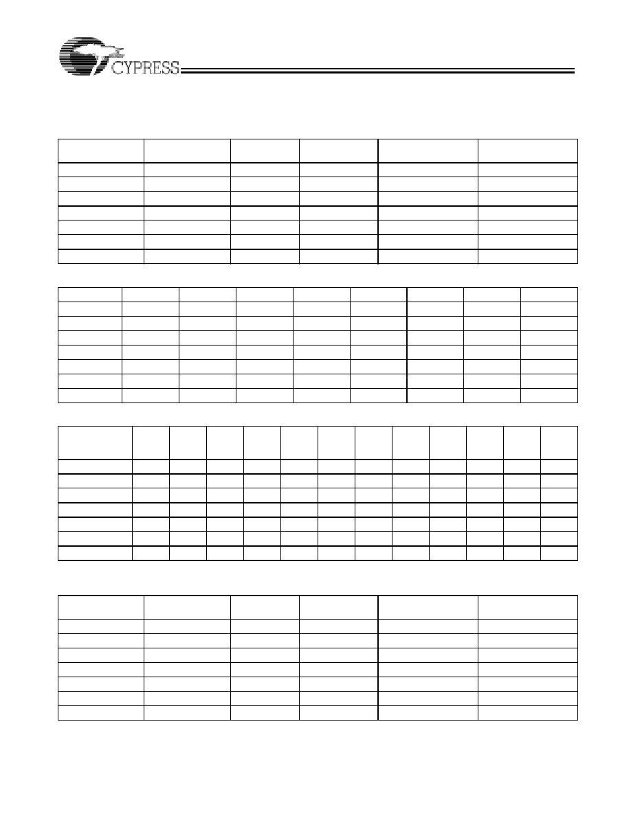
Selection Guide
5.0V Selection Guide
3.3V Selection Guide
General Information
Device
Macrocells
Dedicated
Inputs
I/O Pins
Speed (t
PD
)
Speed (f
MAX
)
CY37032
32
5
32
6
200
CY37064
64
5
32/64
6
200
CY37128
128
5
64/128
6.5
167
CY37192
192
5
120
7.5
154
CY37256
256
5
128/160/192
7.5
154
CY37384
384
5
160/192
10
118
CY37512
512
5
160/192/264
10
118
Speed Bins
Device
200
167
154
143
125
100
83
66
CY37032
X
X
X
CY37064
X
X
X
CY37128
X
X
X
CY37192
X
X
X
CY37256 X
X
X
CY37384
X
X
CY37512
X
X
X
Device-Package Offering and I/O Count
Device
44-
Lead
TQFP
44-
Lead
PLCC
44-
Lead
CLCC
84-
Lead
PLCC
84-
Lead
CLCC
100-
Lead
TQFP
160-
Lead
TQFP
160-
Lead
CQFP
208-
Lead
PQFP
208-
Lead
CQFP
256-
Lead
BGA
352-
Lead
BGA
CY37032
37
37
CY37064
37
37
37
69
69
CY37128
69
69
69
133
CY37192
125
CY37256
133
133
165
197
CY37384
165
197
CY37512
165
165
197
269
General Information
Device
Macrocells
Dedicated
Inputs
I/O Pins
Speed (t
PD
)
Speed (f
MAX
)
CY37032V
32
5
32
8.5
143
CY37064V
64
5
32/64
8.5
143
CY37128V
128
5
64/80/128
10
125
CY37192V
192
5
120
12
100
CY37256V
256
5
128/160/192
12
100
CY37384V
384
5
160/192
15
83
CY37512V
512
5
160/192/264
15
83
Ultra37000 CPLD Family
Document #: 38-03007 Rev. *B
Page 3 of 63
Architecture Overview of Ultra37000 Family
Programmable Interconnect Matrix
The Programmable Interconnect Matrix (PIM) consists of a
completely global routing matrix for signals from I/O pins and
feedbacks from the logic blocks. The PIM provides extremely
robust interconnection to avoid fitting and density limitations.
The inputs to the PIM consist of all I/O and dedicated input pins
and all macrocell feedbacks from within the logic blocks. The
number of PIM inputs increases with pin count and the number
of logic blocks. The outputs from the PIM are signals routed to
the appropriate logic blocks. Each logic block receives 36
inputs from the PIM and their complements, allowing for 32-bit
operations to be implemented in a single pass through the
device. The wide number of inputs to the logic block also
improves the routing capacity of the Ultra37000 family.
An important feature of the PIM is its simple timing. The propa-
gation delay through the PIM is accounted for in the timing
specifications for each device. There is no additional delay for
traveling through the PIM. In fact, all inputs travel through the
PIM. As a result, there are no route-dependent timing param-
eters on the Ultra37000 devices. The worst-case PIM delays
are incorporated in all appropriate Ultra37000 specifications.
Routing signals through the PIM is completely invisible to the
user. All routing is accomplished by software--no hand routing
is necessary. WarpTM and third-party development packages
automatically route designs for the Ultra37000 family in a
matter of minutes. Finally, the rich routing resources of the
Ultra37000 family accommodate last minute logic changes
while maintaining fixed pin assignments.
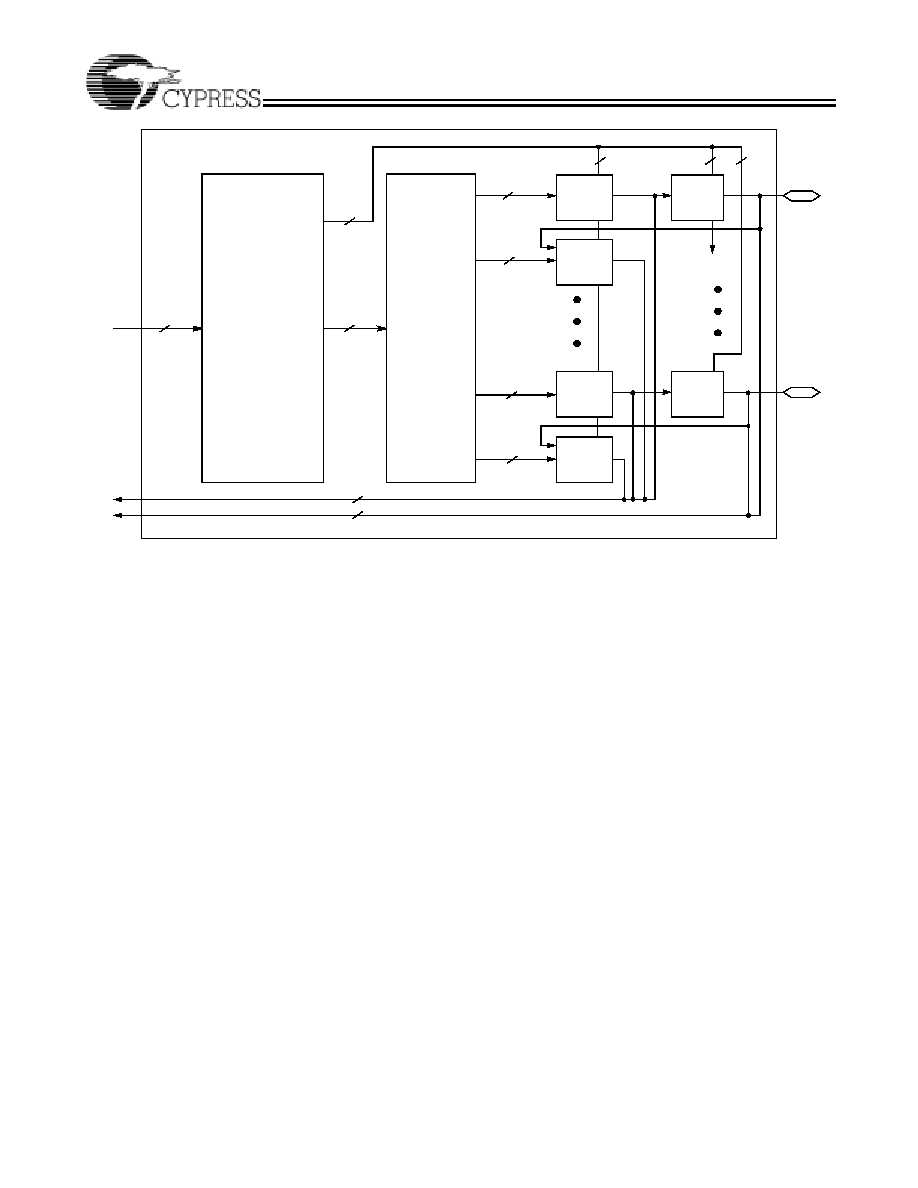
Logic Block
The logic block is the basic building block of the Ultra37000
architecture. It consists of a product term array, an intelligent
product-term allocator, 16 macrocells, and a number of I/O
cells. The number of I/O cells varies depending on the device
used. Refer to Figure 1 for the block diagram.
Product Term Array
Each logic block features a 72 x 87 programmable product
term array. This array accepts 36 inputs from the PIM, which
originate from macrocell feedbacks and device pins. Active
LOW and active HIGH versions of each of these inputs are
generated to create the full 72-input field. The 87 product
terms in the array can be created from any of the 72 inputs.
Of the 87 product terms, 80 are for general-purpose use for
the 16 macrocells in the logic block. Four of the remaining
seven product terms in the logic block are output enable (OE)
product terms. Each of the OE product terms controls up to
eight of the 16 macrocells and is selectable on an individual
macrocell basis. In other words, each I/O cell can select
between one of two OE product terms to control the output
buffer. The first two of these four OE product terms are
available to the upper half of the I/O macrocells in a logic block.
The other two OE product terms are available to the lower half
of the I/O macrocells in a logic block.
The next two product terms in each logic block are dedicated
asynchronous set and asynchronous reset product terms. The
final product term is the product term clock. The set, reset, OE
and product term clock have polarity control to realize OR
functions in a single pass through the array.
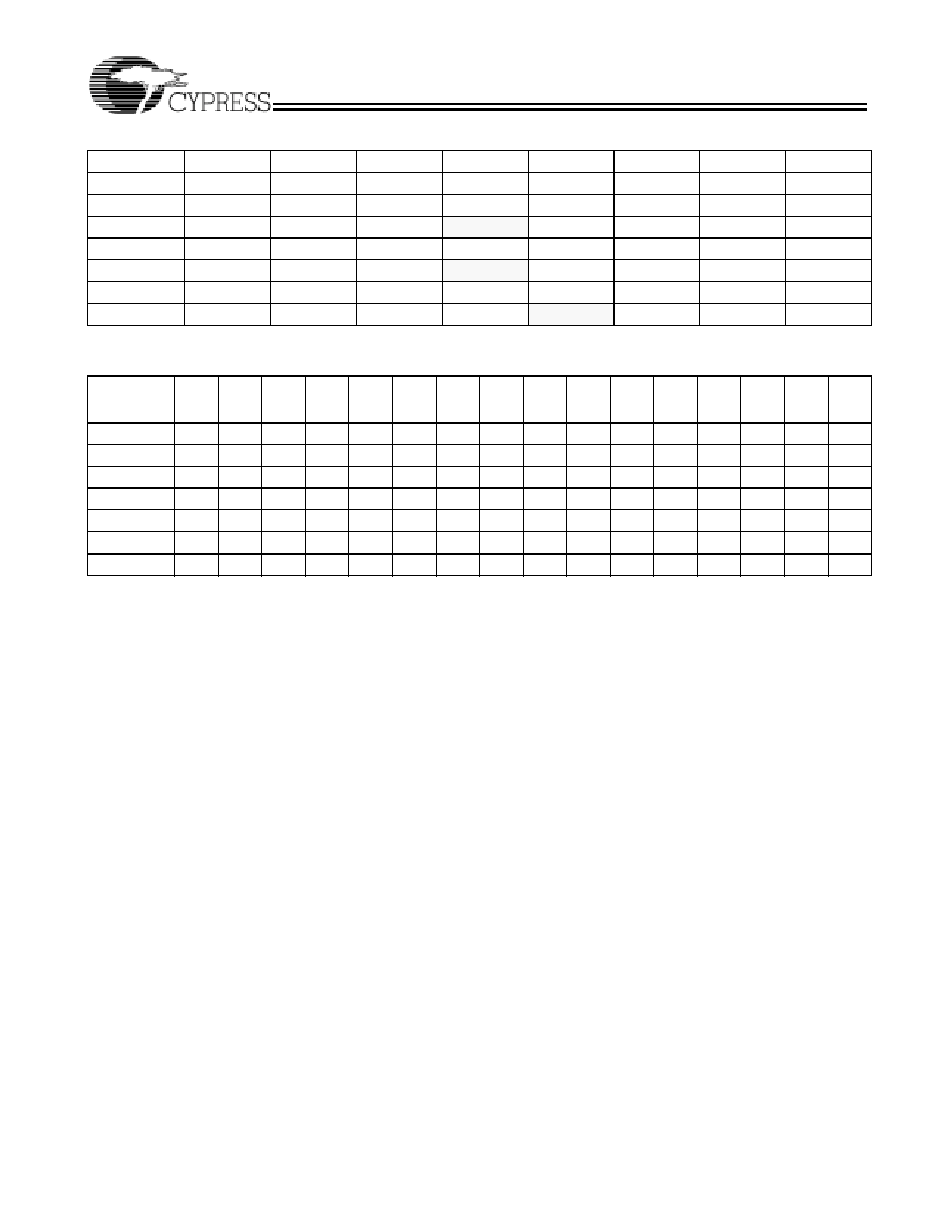
Speed Bins
Device
200
167
154
143
125
100
83
66
CY37032V
X
X
CY37064V
X
X
CY37128V
X
X
X
CY37192V
X
X
CY37256V
X
X
X
CY37384V
X
X
CY37512V
X
X
X
Shaded areas indicate preliminary speed bins.
Device-Package Offering & I/O Count
Device
44
-
Le
ad
TQ
FP
44
-
Le
ad
PLCC
44
-
Le
ad
CLCC
48
-
Le
ad
FBG
A
84
-
Le
ad
PLCC
84
-
Le
ad
CLCC
100
-
Le
ad
TQ
FP
100
-
Le
ad
FBG
A
160
-
Le
ad
TQ
FP
160
-
Le
ad
CQ
F
P
208
-
Le
ad
PQFP
208
-
Le
ad
CQ
F
P
256
-
Le
ad
BGA
256
-
Le
ad
FBG
A
352
-
Le
ad
BGA
400
-
Le
ad
FBG
A
CY37032V
37
37
37
CY37064V
37
37
37
37
69
69
69
CY37128V
69
69
69
85
133
CY37192V
125
CY37256V
133
133
165
197
197
CY37384V
165
197
CY37512V
165
165
197
269
269
Ultra37000 CPLD Family
Document #: 38-03007 Rev. *B
Page 4 of 63
Low-Power Option
Each logic block can operate in high-speed mode for critical
path performance, or in low-power mode for power conser-
vation. The logic block mode is set by the user on a logic block
by logic block basis.
Product Term Allocator
Through the product term allocator, software automatically
distributes product terms among the 16 macrocells in the logic
block as needed. A total of 80 product terms are available from
the local product term array. The product term allocator
provides two important capabilities without affecting perfor-
mance: product term steering and product term sharing.
Product Term Steering
Product term steering is the process of assigning product
terms to macrocells as needed. For example, if one macrocell
requires ten product terms while another needs just three, the
product term allocator will "steer" ten product terms to one
macrocell and three to the other. On Ultra37000 devices,
product terms are steered on an individual basis. Any number
between 0 and 16 product terms can be steered to any
macrocell. Note that 0 product terms is useful in cases where
a particular macrocell is unused or used as an input register.
Product Term Sharing
Product term sharing is the process of using the same product
term among multiple macrocells. For example, if more than
one output has one or more product terms in its equation that
are common to other outputs, those product terms are only
programmed once. The Ultra37000 product term allocator
allows sharing across groups of four output macrocells in a
variable fashion. The software automatically takes advantage
of this capability--the user does not have to intervene.
Note that neither product term sharing nor product term
steering have any effect on the speed of the product. All worst-
case steering and sharing configurations have been incorpo-
rated in the timing specifications for the Ultra37000 devices.
Ultra37000 Macrocell
Within each logic block there are 16 macrocells. Macrocells
can either be I/O Macrocells, which include an I/O Cell which
is associated with an I/O pin, or buried Macrocells, which do
not connect to an I/O. The combination of I/O Macrocells and
buried Macrocells varies from device to device.
Buried Macrocell
Figure 2 displays the architecture of buried macrocells. The
buried macrocell features a register that can be configured as
combinatorial, a D flip-flop, a T flip-flop, or a level-triggered
latch.
The register can be asynchronously set or asynchronously
reset at the logic block level with the separate set and reset
product terms. Each of these product terms features program-
mable polarity. This allows the registers to be set or reset
based on an AND expression or an OR expression.
Clocking of the register is very flexible. Four global
synchronous clocks and a product term clock are available to
clock the register. Furthermore, each clock features program-
mable polarity so that registers can be triggered on falling as
well as rising edges (see the Clocking section). Clock polarity
is chosen at the logic block level.
The buried macrocell also supports input register capability.
The buried macrocell can be configured to act as an input
Figure 1. Logic Block with 50% Buried Macrocells
I/O
CELL
0
PRODUCT
TERM
ALLOCATOR
I/O
CELL
14
MACRO-
CELL
0
MACRO-
CELL
1
MACRO-
CELL
14
0
-
16
PRODUCT
TERMS
72 x 87
PRODUCT TERM
ARRAY
80
36
8
16
TO
PIM
FROM
PIM
7
3
2
MACRO-
CELL
15
2
to cells
2, 4, 6 8, 10, 12
0
-
16
PRODUCT
TERMS
0
-
16
PRODUCT
TERMS
0
-
16
PRODUCT
TERMS

Ultra37000 CPLD Family
Document #: 38-03007 Rev. *B
Page 5 of 63
register (D-type or latch) whose input comes from the I/O pin
associated with the neighboring macrocell. The output of all
buried macrocells is sent directly to the PIM regardless of its
configuration.
I/O Macrocell
Figure 2 illustrates the architecture of the I/O macrocell. The
I/O macrocell supports the same functions as the buried
macrocell with the addition of I/O capability. At the output of the
macrocell, a polarity control mux is available to select active
LOW or active HIGH signals. This has the added advantage
of allowing significant logic reduction to occur in many appli-
cations.
The Ultra37000 macrocell features a feedback path to the PIM
separate from the I/O pin input path. This means that if the
macrocell is buried (fed back internally only), the associated
I/O pin can still be used as an input.
Bus Hold Capabilities on all I/Os
Bus-hold, which is an improved version of the popular internal
pull-up resistor, is a weak latch connected to the pin that does
not degrade the device's performance. As a latch, bus-hold
maintains the last state of a pin when the pin is placed in a
high-impedance state, thus reducing system noise in bus-
interface applications. Bus-hold additionally allows unused
device pins to remain unconnected on the board, which is
particularly useful during prototyping as designers can route
new signals to the device without cutting trace connections to
V
CC
or GND. For more information, see the application note
"Understanding Bus-Hold - A Feature of Cypress CPLDs."
Programmable Slew Rate Control
Each output has a programmable configuration bit, which sets
the output slew rate to fast or slow. For designs concerned with
meeting FCC emissions standards the slow edge provides for
lower system noise. For designs requiring very high perfor-
mance the fast edge rate provides maximum system perfor-
mance.