 | –≠–ª–µ–∫—Ç—Ä–æ–Ω–Ω—ã–π –∫–æ–º–ø–æ–Ω–µ–Ω—Ç: W150H | –°–∫–∞—á–∞—Ç—å:  PDF PDF  ZIP ZIP |
PRELIMINARY
440BX AGPset Spread Spectrum
Frequency Synthesizer
W150
Cypress Semiconductor Corporation
∑
3901 North First Street
∑
San Jose
,
CA 95134
∑
408-943-2600
Document #: 38-07177 Rev. *B
Revised January 27, 2003
Features
∑ Maximized electromagnetic interference (EMI)
suppression using Cypress's Spread Spectrum
technology
∑ Single-chip system frequency synthesizer for Intel
Æ
440BX AGPset
∑ Three copies of CPU output
∑ Seven copies of PCI output
∑ One 48-MHz output for USB/one 24-MHz for SIO
∑ Two buffered reference outputs
∑ Two IOAPIC outputs
∑ 17 SDRAM outputs provide support for four DIMMs
∑ Supports frequencies up to 150 MHz
∑ SMBus interface for programming
∑ Power management control inputs
Key Specifications
CPU Cycle-to-Cycle Jitter: .......................................... 250 ps
CPU to CPU Output Skew: ......................................... 175 ps
PCI to PCI Output Skew:............................................. 500 ps
SDRAMIN to SDRAM0:15 Delay:.......................... 3.7 ns typ.
V
DDQ3
: ..................................................................... 3.3V±5%
V
DDQ2
: ..................................................................... 2.5V±5%
SDRAM0:15 (leads) to SDRAM_F Skew: ............. 0.4 ns typ.
Table 1. Mode Input Table
Mode
Pin 3
0
PCI_STOP#
1
REF0
Table 2. Pin Selectable Frequency
Input Address
CPU_F, 1:2
(MHz)
PCI_F, 0:5
(MHz)
FS3
FS2
FS1
FS0
1
1
1
1
133.3
33.3 (CPU/4)
1
1
1
0
124
31 (CPU/4)
1
1
0
1
150
37.5 (CPU/4)
1
1
0
0
140
35 (CPU/4)
1
0
1
1
105
35 (CPU/3)
1
0
1
0
110
36.7 (CPU/3)
1
0
0
1
115
38.3 (CPU/3)
1
0
0
0
120
40 (CPU/3)
0
1
1
1
100
33.3 (CPU/3)
0
1
1
0
133.3
44.43 (CPU/3)
0
1
0
1
112
37.3 (CPU/3)
0
1
0
0
103
34.3 (CPU/3)
0
0
1
1
66.8
33.4 (CPU/2)
0
0
1
0
83.3
41.7 (CPU/2)
0
0
0
1
75
37.5 (CPU/2)
0
0
0
0
124
41.3 (CPU/3)
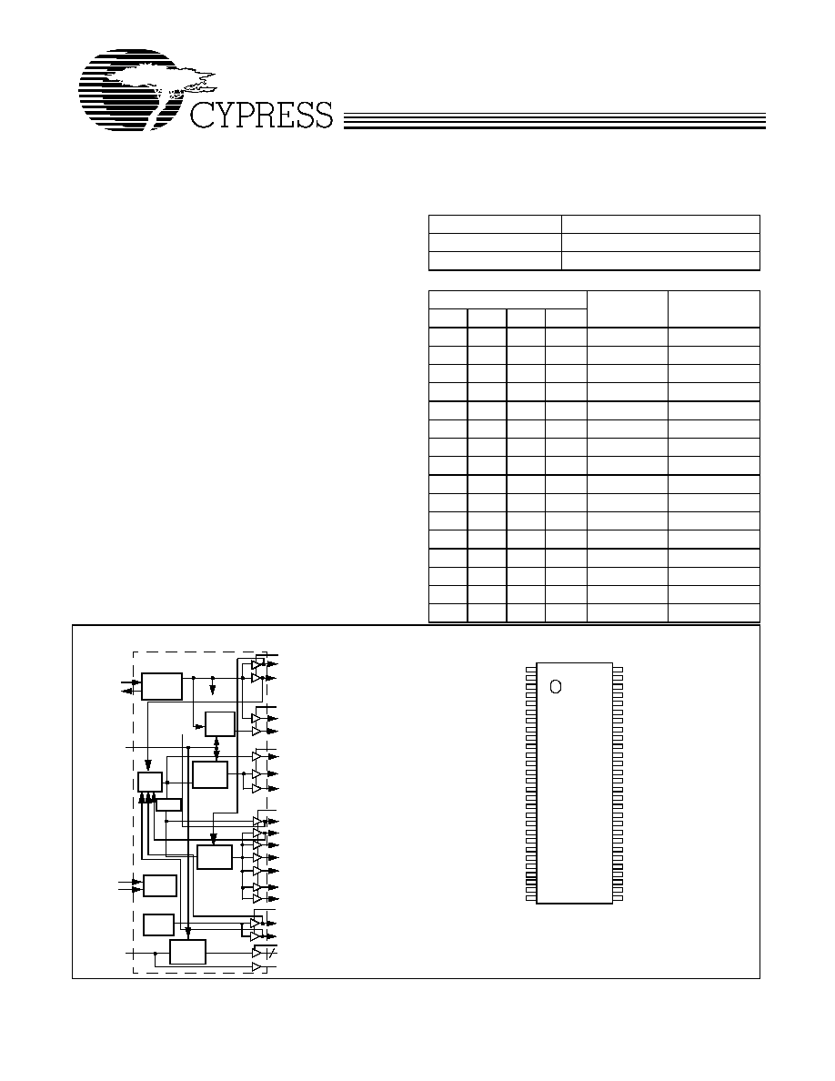
Logic Block Diagram
Pin Configuration
[1]
VDDQ3
REF0/(PCI_STOP#)
VDDQ2
IOAPIC_F
CPU_F
CPU1
CPU2
PCI_F/MODE
XTAL
PLL Ref Freq
PLL 1
X2
X1
REF1/FS2
VDDQ3
Stop
Clock
Control
Stop
Clock
Control
PCI1
PCI2
PCI3
PCI5
48MHz/FS1
24MHz/FS0
PLL2
˜2,3,4
OSC
VDDQ2
CLK_STOP#
VDDQ3
IOAPIC0
PCI4
SMBus
SDATA
Logic
SCLK
I/O Pin
Control
SDRAM0:15
SDRAMIN
16
VDDQ3
PCI0/FS3
Stop
Clock
Control
Stop
Clock
Control
SDRAM_F
VDDQ3
REF1/FS2
REF0/(PCI_STOP#)
GND
X1
X2
VDDQ3
PCI_F/MODE
PCI0/FS3
GND
PCI1
PCI2
PCI3
PCI4
VDDQ3
PCI5
SDRAMIN
SDRAM11
SDRAM10
VDDQ3
SDRAM9
SDRAM8
GND
SDRAM15
W1
5
0
VDDQ2
IOAPIC0
IOAPIC_F
GND
CPU_F
CPU1
VDDQ2
CPU2
GND
CLK_STOP#
SDRAM_F
VDDQ3
SDRAM0
SDRAM1
GND
SDRAM2
SDRAM3
SDRAM4
SDRAM5
VDDQ3
SDRAM6
SDRAM7
GND
SDRAM12
56
55
54
53
52
51
50
49
48
47
46
45
44
43
42
41
40
39
38
37
36
35
34
33
1
2
3
4
5
6
7
8
9
10
11
12
13
14
15
16
17
18
19
20
21
22
23
24
25
26
27
28
32
31
30
29
SDRAM14
GND
SDATA
SCLK
SDRAM13
VDDQ3
24MHz/FS0
48MHz/FS1
Note:
1.
1.Internal pull-up resistors should not be relied upon for setting I/O pins HIGH. Pin function
with parentheses determined by MODE pin resistor strapping. Unlike other I/O pins, input
FS3 has an internal pull-down resistor.
PRELIMINARY
W150
Document #: 38-07177 Rev. *B
Page 2 of 15
Pin Definitions
Pin Name
Pin No.
Pin
Type
Pin Description
CPU1:2
51, 49
O
CPU Outputs 1 and 2: Frequency is set by the FS0:3 inputs or through serial input interface,
see Table 2 and Table 6. These outputs are affected by the CLK_STOP# input.
CPU_F
52
O
Free-Running CPU Output: Frequency is set by the FS0:3 inputs or through serial input
interface, see Table 2 and Table 6. This output is not affected by the CLK_STOP# input.
PCI1:5
11, 12, 13,
14, 16
O
PCI Outputs 1 through 5: Frequency is set by the FS0:3 inputs or through serial input
interface, see Table 2 and Table 6. These outputs are affected by the PCI_STOP# input.
PCI0/FS3
9
I/O
PCI Output/Frequency Select Input: As an output, frequency is set by the FS0:3 inputs or
through serial input interface, see Table 2 and Table 6. This output is affected by the
PCI_STOP# input. When an input, latches data selecting the frequency of the CPU and PCI outputs.
PCI_F/MODE
8
I/O
Free Running PCI Output: Frequency is set by the FS0:3 inputs or through serial input
interface, see Table 2 and Table 6. This output is not affected by the PCI_STOP# input. When
an input, selects function of pin 3 as described in Table 1.
CLK_STOP#
47
I
CLK_STOP# Input: When brought LOW, affected outputs are stopped LOW after completing
a full clock cycle (2≠3 CPU clock latency). When brought HIGH, affected outputs start
beginning with a full clock cycle (2≠3 CPU clock latency).
IOAPIC_F
54
O
Free-running IOAPIC Output: This output is a buffered version of the reference input which
is not affected by the CPU_STOP# logic input. Its swing is set by voltage applied to VDDQ2.
IOAPIC0
55
O
IOAPIC Output: Provides 14.318-MHz fixed frequency. The output voltage swing is set by
voltage applied to VDDQ2. This output is disabled when CLK_STOP# is set LOW.
48MHz/FS1
29
I/O
48-MHz Output: 48 MHz is provided in normal operation. In standard systems, this output can
be used as the reference for the Universal Serial Bus. Upon power up, FS1 input will be
latched, setting output frequencies as described in Table 2.
24MHz/FS0
30
I/O
24-MHz Output: 24 MHz is provided in normal operation. In standard systems, this output can
be used as the clock input for a Super I/O chip. Upon power up, FS0 input will be latched,
setting output frequencies as described in Table 2.
REF1/FS2
2
I/O
Reference Output: 14.318 MHz is provided in normal operation. Upon power-up, FS2 input
will be latched, setting output frequencies as described in Table 2.
REF0
(PCI_STOP#)
3
I/O
Fixed 14.318-MHz Output 0 or PCI_STOP# Pin: Function determined by MODE pin. The
PCI_STOP# input enables the PCI 0:5 outputs when HIGH and causes them to remain at logic
0 when LOW. The PCI_STOP signal is latched on the rising edge of PCI_F. Its effects take
place on the next PCI_F clock cycle. As an output, this pin provides a fixed clock signal equal
in frequency to the reference signal provided at the X1/X2 pins (14.318 MHz).
SDRAMIN
17
I
Buffered Input Pin: The signal provided to this input pin is buffered to 17 outputs
(SDRAM0:15, SDRAM_F).
SDRAM0:15
44, 43,
41, 40,
39, 38,
36, 35,
22, 21,
19, 18,
33, 32,
25, 24
O
Buffered Outputs: These sixteen dedicated outputs provide copies of the signal provided at
the SDRAMIN input. The swing is set by VDDQ3, and they are deactivated when CLK_STOP#
input is set LOW.
SDRAM_F
46
O
Free-Running Buffered Output: This output provides a single copy of the SDRAMIN input.
The swing is set by VDDQ3; this signal is unaffected by the CLK_STOP# input.
SCLK
28
I
Clock pin for SMBus circuitry.
SDATA
27
I/O
Data pin for SMBus circuitry.
X1
5
I
Crystal Connection or External Reference Frequency Input: This pin has dual functions.
It can be used as an external 14.318 MHz crystal connection or as an external reference
frequency input.
X2
6
I
Crystal Connection: An input connection for an external 14.318-MHz crystal. If using an
external reference, this pin must be left unconnected.
VDDQ3
1, 7, 15,
20, 31,
37, 45
P
Power Connection: Power supply for core logic, PLL circuitry, SDRAM output buffers, PCI
output buffers, reference output buffers, and 48-MHz/24-MHz output buffers. Connect to 3.3V.
PRELIMINARY
W150
Document #: 38-07177 Rev. *B
Page 3 of 15
Overview
The W150 was designed as a single-chip alternative to the
standard two-chip Intel 440BX AGPset clock solution. It
provides sufficient outputs to support most single-processor,
four SDRAM DIMM designs.
Functional Description
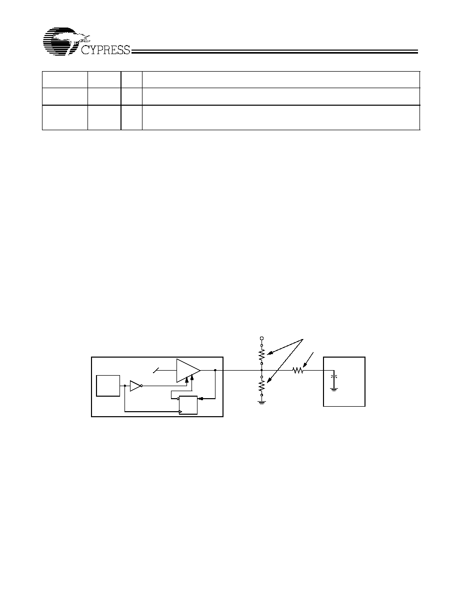
I/O Pin Operation
Pins 2, 8, 9, 29, and 30 are dual-purpose l/O pins. Upon
power-up these pins act as logic inputs, allowing the determi-
nation of assigned device functions. A short time after
power-up, the logic state of each pin is latched and the pins
become clock outputs. This feature reduces device pin count
by combining clock outputs with input select pins.
An external 10-k
"strapping" resistor is connected between
the l/O pin and ground or V
DD
. Connection to ground sets a
latch to "0," connection to V
DD
sets a latch to "1." Figure 1 and
Figure 2 show two suggested methods for strapping resistor
connections.
Upon W150 power-up, the first 2 ms of operation are used for
input logic selection. During this period, the five I/O pins (2, 8,
9, 29, 30) are three-stated, allowing the output strapping
resistor on the l/O pins to pull the pins and their associated
capacitive clock load to either a logic HIGH or LOW state. At
the end of the 2-ms period, the established logic "0" or "1"
condition of the l/O pin is latched. Next the output buffer is
enabled, converting the l/O pins into operating clock outputs.
The 2-ms timer starts when V
DD
reaches 2.0V. The input bits
can only be reset by turning V
DD
off and then back on again.
It should be noted that the strapping resistors have no signif-
icant effect on clock output signal integrity. The drive
impedance of clock output (< 40
, nominal) is minimally
affected by the 10-k
strap to ground or V
DD
. As with the
series termination resistor, the output strapping resistor should
be placed as close to the l/O pin as possible in order to keep
the interconnecting trace short. The trace from the resistor to
ground or V
DD
should be kept less than two inches in length
to minimize system noise coupling during input logic sampling.
When the clock outputs are enabled following the 2-ms input
period, the corresponding specified output frequency is
delivered on the pins, assuming that V
DD
has stabilized. If V
DD
has not yet reached full value, output frequency initially may
be below target but will increase to target once V
DD
voltage
has stabilized. In either case, a short output clock cycle may
be produced from the CPU clock outputs when the outputs are
enabled.
VDDQ2
50, 56
P
Power Connection: Power supply for IOAPIC and CPU output buffers. Connect to 2.5V or
3.3V.
GND
4, 10, 23,
26, 34,
42, 48, 53
G
Ground Connections: Connect all ground pins to the common system ground plane.
Pin Definitions
(continued)
Pin Name
Pin No.
Pin
Type
Pin Description
Power-on
Reset
Timer
Output Three-state
Data
Latch
Hold
Q
D
W150
V
DD
Clock Load
10 k
Output
Buffer
(Load Option 1)
10 k
(Load Option 0)
Output
Low
Output Strapping Resistor
Series Termination Resistor
Figure 1. Input Logic Selection Through Resistor Load Option
PRELIMINARY
W150
Document #: 38-07177 Rev. *B
Page 4 of 15
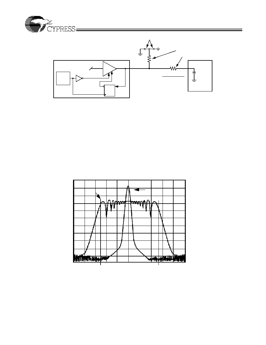
Spread Spectrum Generator
The device generates a clock that is frequency modulated in
order to increase the bandwidth that it occupies. By increasing
the bandwidth of the fundamental and its harmonics, the ampli-
tudes of the radiated electromagnetic emissions are reduced.
This effect is depicted in Figure 3.
As shown in Figure 3, a harmonic of a modulated clock has a
much lower amplitude than that of an unmodulated signal. The
reduction in amplitude is dependent on the harmonic number
and the frequency deviation or spread. The equation for the
reduction is
dB = 6.5 + 9*log10(P) + 9*log10(F)
Where P is the percentage of deviation and F is the frequency
in MHz where the reduction is measured.
The output clock is modulated with a waveform depicted in
Figure 4. This waveform, as discussed in "Spread Spectrum
Clock Generation for the Reduction of Radiated Emissions" by
Bush, Fessler, and Hardin produces the maximum reduction
in the amplitude of radiated electromagnetic emissions. The
deviation selected for this chip is specified in Table 6. Figure 4
details the Cypress spreading pattern. Cypress does offer
options with more spread and greater EMI reduction. Contact
your local Sales representative for details on these devices.
Spread Spectrum clocking is activated or deactivated by
selecting the appropriate values for bits 1≠0 in data byte 0 of
the SMBus data stream. Refer to Table 7 for more details.
Power-on
Reset
Timer
Output Three-state
Data
Latch
Hold
Q
D
W150
V
DD
Clock Load
R
10 k
Output
Buffer
Output
Low
Output Strapping Resistor
Series Termination Resistor
Jumper Options
Resistor Value R
Figure 2. Input Logic Selection Through Jumper Option
Figure 3. Clock Harmonic with and without SSCG Modulation Frequency Domain Representation
SSFTG
Typical Clock
Frequency Span (MHz)
≠1.0
+1.0
0
≠0.5%
≠SS%
+SS%
A
m
pl
itude (
d
B
)
5 dB/div
+0.5%

PRELIMINARY
W150
Document #: 38-07177 Rev. *B
Page 5 of 15
Serial Data Interface
The W150 features a two-pin, serial data interface that can be
used to configure internal register settings that control
particular device functions. Upon power-up, the W150
initializes with default register settings, therefore the use of this
serial data interface is optional. The serial interface is
write-only (to the clock chip) and is the dedicated function of
device pins SDATA and SCLOCK. In motherboard applica-
tions, SDATA and SCLOCK are typically driven by two logic
outputs of the chipset. If needed, clock device register
changes are normally made upon system initialization. The
interface can also be used during system operation for power
management functions. Table 3 summarizes the control
functions of the serial data interface.
Operation
Data is written to the W150 in eleven bytes of eight bits each.
Bytes are written in the order shown in Table 4.
MAX
MIN
10%
20%
30%
40%
50%
60%
70%
80%
90%
1
00%
10%
20%
30%
40%
50%
60%
70%
80%
90%
1
00%
FREQUENCY
Figure 4. Typical Modulation Profile
Table 3. Serial Data Interface Control Functions Summary
Control Function
Description
Common Application
Clock Output Disable Any individual clock output(s) can be disabled.
Disabled outputs are actively held LOW.
Unused outputs are disabled to reduce EMI and
system power. Examples are clock outputs to
unused PCI slots.
CPU Clock
Frequency Selection
Provides CPU/PCI frequency selections through
software. Frequency is changed in a smooth and
controlled fashion.
For alternate microprocessors and power
management options. Smooth frequency transition
allows CPU frequency change under normal system
operation.
Spread Spectrum
Enabling
Enables or disables spread spectrum clocking.
For EMI reduction.
Output Three-state
Puts clock output into a high-impedance state.
Production PCB testing.
Test Mode
All clock outputs toggle in relation to X1 input,
internal PLL is bypassed. Refer to Table 5.
Production PCB testing.
(Reserved)
Reserved function for future device revision or
production device testing.
No user application. Register bit must be written as
0.
Table 4. Byte Writing Sequence
Byte
Sequence
Byte Name
Bit Sequence
Byte Description
1
Slave Address 11010010
Commands the W150 to accept the bits in Data Bytes 0≠7 for internal register
configuration. Since other devices may exist on the same common serial data bus,
it is necessary to have a specific slave address for each potential receiver. The
slave receiver address for the W150 is 11010010. Register setting will not be made
if the Slave Address is not correct (or is for an alternate slave receiver).
2
Command
Code
Don't Care
Unused by the W150, therefore bit values are ignored ("Don't Care"). This byte
must be included in the data write sequence to maintain proper byte allocation. The
Command Code Byte is part of the standard serial communication protocol and
may be used when writing to another addressed slave receiver on the serial data
bus.
3
Byte Count
Don't Care
Unused by the W150, therefore bit values are ignored ("Don't Care"). This byte
must be included in the data write sequence to maintain proper byte allocation. The
Byte Count Byte is part of the standard serial communication protocol and may be
used when writing to another addressed slave receiver on the serial data bus.