 | –≠–ª–µ–∫—Ç—Ä–æ–Ω–Ω—ã–π –∫–æ–º–ø–æ–Ω–µ–Ω—Ç: W152-11X | –°–∫–∞—á–∞—Ç—å:  PDF PDF  ZIP ZIP |
Spread AwareTM, Eight Output Zero Delay Buffer
W152
Cypress Semiconductor Corporation
∑
3901 North First Street
∑
San Jose
∑
CA 95134
∑
408-943-2600
Document #: 38-07148 Rev. *A
Revised December 14, 02
Features
∑ Spread AwareTM--designed to work with SSFTG
reference signals
∑ Two banks of four outputs each
∑ Configuration options to halve, double, or quadruple
the reference frequency refer to Table 1 to determine
the specific option which meets your multiplication
needs
∑ Outputs may be three-stated
∑ Available in 16-pin SOIC package
∑ Extra strength output drive available (-11/-12 versions)
∑ Contact factory for availability information on 16-pin
TSSOP
Key Specifications
Operating Voltage: ............................................... 3.3V±10%
Operating Range: ................... 15 MHz < f
OUTQA
< 140 MHz
Cycle-to-Cycle Jitter: (Refer to Figure 3) .................... 225 ps
Cycle-to-Cycle Jitter: Frequency Range
25 to140 MHz ......................................................... 125 ps
Output to Output Skew: Between Banks ..................... 215 ps
Output to Output Skew: Within Banks
(Refer to Figure 4) ................................................... 100 ps
Total Timing Budget Impact: ........................................ 555 ps
Max. Phase Error Variation:.......................................±225 ps
Tracking Skew: ..........................................................±130 ps
Table 1. Configuration Options
Device
Feedback Signal
QA0:3
QB0:3
W152-1/11
[1]
QA0:3 or QB0:3
REFx1
REFx1
W152-2/12
[2]
QA0:3
REFx1
REF/2
W152-2/12
[2]
QB0:3
REFx2
REFx1
W152-3
QA0:3
REFx2
REFx1
W152-3
QB0:3
REFx4
REFx2
W152-4
QA0:3 or QB0:3
REFx2
REFx2
Notes:
1.
W152-11 has stronger output drive than the W152-1.
2.
W152-12 has stronger output drive than the W152-2.
Spread Aware is a trademark of Cypress Semiconductor Corporation.
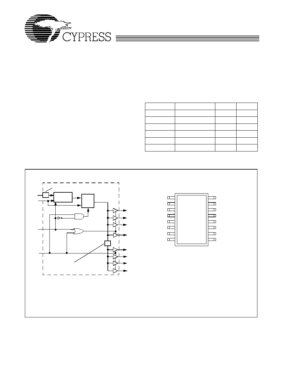
Block Diagram
Pin Configuration
QA0
PLL
REF
MUX
QA1
QA2
QA3
QB0
QB1
˜2
SEL0
FBIN
QB2
QB3
SEL1
˜2
(present on the -3 and -4 only)
(present on the -2, -12, and -3 only)
FBIN
QA3
QA2
VDD
GND
QB3
QB2
SEL0
16
15
14
13
12
11
10
9
REF
QA0
QA1
VDD
GND
QB0
QB1
SEL1
1
2
3
4
5
6
7
8
W152
Document #: 38-07148 Rev. *A
Page 2 of 8
Overview
The W152 products are eight-output zero delay buffers. A
Phase-Locked Loop (PLL) is used to take a time-varying signal
and provide eight copies of that same signal out. The external
feedback to the PLL provides outputs in phase with the refer-
ence inputs.
Internal dividers exist in some options allowing the user to get
a simple multiple (/2, x2, x4) of the reference input, for details
see Table 1. Because the outputs are separated into two
banks, it is possible to provide some combination of these mul-
tiples at the same time.
Spread Aware
Many systems being designed now utilize a technology called
Spread Spectrum Frequency Timing Generation. Cypress has
been one of the pioneers of SSFTG development, and we de-
signed this product so as not to filter off the Spread Spectrum
feature of the Reference input, assuming it exists. When a
zero delay buffer is not designed to pass the SS feature
through, the result is a significant amount of tracking skew
which may cause problems in systems requiring synchroniza-
tion.
For more details on Spread Spectrum timing technology,
please see the Cypress application note titled, "EMI Suppres-
sion Techniques with Spread Spectrum Frequency Timing
Generator (SSFTG) ICs."
Functional Description
Logic inputs provide the user the ability to turn off one or both
banks of clocks when not in use, as described in Table 2. Dis-
abling a bank of unused outputs will reduce jitter and power
consumption, and will also reduce the amount of EMI gener-
ated by the W152.
These same inputs allow the user to bypass the PLL entirely
if so desired. When this is done, the device no longer acts as
a zero delay buffer, it simply reverts to a standard eight-output
clock driver.
The W152 PLL enters an auto power-down mode when there
are no rising edges on the REF input. In this mode, all outputs
are three-stated and the PLL is turned off.
Pin Definitions
Pin Name
Pin No.
Pin
Type
Pin Description
REF
1
I
Reference Input: The output signals QA0:3 through QB0:3 will be synchronized to
this signal unless the device is programmed to bypass the PLL.
FBIN
16
I
Feedback Input: When programmed to zero delay buffer mode, this input must be
fed by one of the outputs (QA0:3 or QB0:3) to ensure proper functionality. If the trace
between FBIN and the output pin being used for feedback is equal in length to the
traces between the outputs and the signal destinations, then the signals received at
the destinations will be synchronized to the REF signal input.
QA0:3
2, 3, 14, 15
O
Outputs from Bank A: The frequency of the signals provided by these pins is deter-
mined by the feedback signal connected to FBIN, and the specific W152 option being
used. See Table 2.
QB0:3
6, 7, 10, 11
O
Outputs from Bank B: The frequency of the signals provided by these pins is deter-
mined by the feedback signal connected to FBIN, and the specific W152 option being
used. See Table 2.
VDD
4, 13
P
Power Connections: Connect to 3.3V. Use ferrite beads to help reduce noise for
optimal jitter performance.
GND
5, 12
G
Ground Connections: Connect all grounds to the common system ground plane.
SEL0:1
9, 8
I
Function Select Inputs: Tie to V
DD
(HIGH, 1) or GND (LOW, 0) as desired per
Table 2.
Table 2. Input Logic
SEL1
SEL0
QA0:3
QB0:3
PLL
0
0
Three-State Three-State
Shutdown
0
1
Active
Three-State
Active, Utilized
1
0
Active
Active
Shutdown,
Bypassed
1
1
Active
Active
Active, Utilized
W152
Document #: 38-07148 Rev. *A
Page 3 of 8
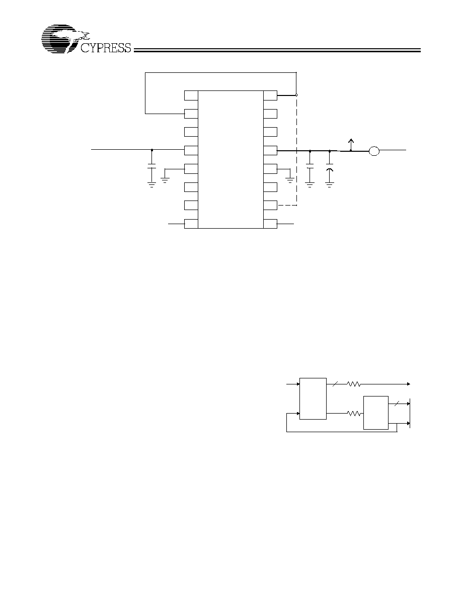
How to Implement Zero Delay
Typically, zero delay buffers (ZDBs) are used because a de-
signer wants to provide multiple copies of a clock signal in
phase with each other. The whole concept behind ZDBs is that
the signals at the destination chips are all going HIGH at the
same time as the input to the ZDB. In order to achieve this,
layout must compensate for trace length between the ZDB and
the target devices. The method of compensation is described
below.
External feedback is the trait that allows for this compensation.
The PLL on the ZDB will cause the feedback signal to be in
phase with the reference signal. When laying out the board,
match the trace lengths between the output being used for
feedback and the FBIN input to the PLL.
If it is desirable to either add a little delay, or slightly precede
the input signal, this may also be affected by either making the
trace to the FBIN pin a little shorter or a little longer than the
traces to the devices being clocked.
Inserting Other Devices in Feedback Path
Another nice feature available due to the external feedback is
the ability to synchronize signals up to the signal coming from
some other device. This implementation can be applied to any
device (ASIC, multiple output clock buffer/driver, etc.) which is
put into the feedback path.
Referring to Figure 2, if the traces between the ASIC/buffer
and the destination of the clock signal(s) (A) are equal in length
to the trace between the buffer and the FBIN pin, the signals
at the destination(s) device will be driven HIGH at the same
time the Reference clock provided to the ZDB goes HIGH.
Synchronizing the other outputs of the ZDB to the outputs form
the ASIC/Buffer is more complex however, as any propagation
delay in the ASIC/Buffer must be accounted for.
9
2
3
1
4
7
6
8
5
16
13
14
15
10
11
12
3.3V
Supply
VDD
0.1
µ
F
0.1
µ
F10
µ
F
Ferrite
Bead
See Note 3
VDD or GND (for desired operation mo
VDD or GND (for desired operation mode)
QA0
QA2
QA1
QA3
Ground
Power
Power
FB In
Ref In
QB1
QB0
QB2
QB3
SEL1
SEL0
Ground
VDD
Figure 1. Schematic
[4]
Note:
3.
Pin 16 needs to be connected to one of the outputs from either bank A or bank B, it should not be connected to both. Pins 2 and 10 are shown here as
examples. None of the outputs should be considered as preferred for the feedback path.
Reference
Signal
Feedback
Input
ASIC/
Buffer
Zero
Delay
Buffer
A
Figure 2. 6 Output Buffer in the Feedback Path
W152
Document #: 38-07148 Rev. *A
Page 4 of 8
Absolute Maximum Ratings
[3]
Stresses greater than those listed in this table may cause per-
manent damage to the device. These represent a stress rating
only. Operation of the device at these or any other conditions
above those specified in the operating sections of this specifi-
cation is not implied. Maximum conditions for extended peri-
ods may affect reliability.
.
Parameter
Description
Rating
Unit
V
DD
, V
IN
Voltage on any pin with respect to GND
≠0.5 to +7.0
V
T
STG
Storage Temperature
≠65 to +150
∞C
T
A
Operating Temperature
0 to +70
∞C
T
B
Ambient Temperature under Bias
≠55 to +125
∞C
P
D
Power Dissipation
0.5
W
DC Electrical Characteristics
: T
A
=0∞C to 70∞C, V
DD
= 3.3V ±10%
Parameter
Description
Test Condition
Min.
Typ.
Max.
Unit
I
DD
Supply Current
Unloaded, 100 MHz
40
mA
V
IL
Input Low Voltage
0.8
V
V
IH
Input High Voltage
2.0
V
V
OL
Output Low Voltage
I
OL
= 12 mA (-11, -12)
I
OL
= 8 mA (-1, -2, -3, -4)
0.4
V
V
OH
Output High Voltage
I
OH
= 12 mA (-11, -12)
I
OH
= 8 mA (-1, -2, -3, -4)
2.4
V
I
IL
Input Low Current
V
IN
= 0V
50
µ
A
I
IH
Input High Current
V
IN
= V
DD
50
µ
A
AC Electrical Characteristics:
T
A
= 0∞C to +70∞C, V
DD
= 3.3V ±10%
Parameter
Description
Test Condition
Min.
Typ.
Max.
Unit
f
IN
Input Frequency
Note 4
15
140
MHz
f
OUT
Output Frequency
15-pF load
[9]
15
140
MHz
t
R
Output Rise Time (-1, -2, -3, -4)
0.8V to 0.8V, 15-pF load
2
2.5
ns
Output Rise Time (-11, -12)
0.8V to 0.8V, 15-pF load
1.5
ns
t
F
Output Fall Time (-1, -2, -3, -4)
2.0V to 0.8V, 15-pF load
2
2.5
ns
Output Rise Time (-11, -12)
2.0V to 0.8V, 20-pF load
1.5
ns
t
ICLKR
Input Clock Rise Time
[5]
4.5
ns
t
ICLKF
Input Clock Fall Time
[5]
4.5
ns
t
PD
FBIN to REF Skew
[6, 7]
350
ps
t
SK
Output to Output Skew
All outputs loaded equally
[11]
215
ps
t
D
Duty Cycle
15-pF load
[8, 9]
45
50
55
%
t
LOCK
PLL Lock Time
Power supply stable
1.0
ms
t
JC
Jitter, Cycle-to-Cycle
Note 10
225
ps
Notes:
3.
Multiple Supplies: The voltage on any input or I/O pin cannot exceed the power pin during power-up. Power supply sequencing is NOT required.
4.
Input frequency is limited by output frequency range and input to output frequency multiplication factor (which is determined by circuit configuration). See
Table 1.
5.
Longer input rise and fall time will degrade skew and jitter performance.
6.
All AC specifications are measured with a 50
transmission line.
7.
Skew is measured at V
DD
/2 on rising edges.
8.
Duty cycle is measured at V
DD
/2.
9.
For the higher drive -11 and -12, the load is 20 pF.
10. For frequencies above 25 MHz CY - CY = 125 ps.
11. Measured across all outputs. Maximum skew between outputs in the same bank is 100 ps.
W152
Document #: 38-07148 Rev. *A
Page 5 of 8
Ordering Information
Ordering Code
Option
Package
Name
Package Type
W152
-1, -11, -2, -12,
-3, -4
G
X
16-pin SOIC (150 mil)
16-pin TSSOP (4.4 mm)
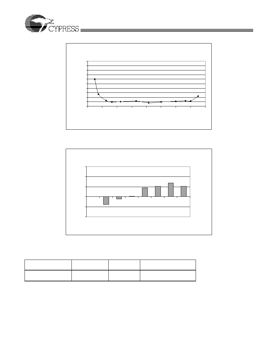
Figure 3. Cycle to Cycle Jitter at 15 pF
W152 -01 CYCLE - CYCLE JITTER @ 15 pF
0
100
200
300
400
500
600
700
800
900
1000
0
20
40
60
80
100
120
140
160
FREQUENCY in MHz
07/21/99 W152-a1
ps
Figure 4. Pin to Pin Skew at 15 pF
W152 -01 PIN- PIN SKEW @ 15 pF
-200
-100
0
100
200
300
A1
A2
A3
A4
B1
B2
B3
B4
OUTPUT #
PIN A1 = REF
O7/21/99 a3
ps