 | –≠–ª–µ–∫—Ç—Ä–æ–Ω–Ω—ã–π –∫–æ–º–ø–æ–Ω–µ–Ω—Ç: W163-15 | –°–∫–∞—á–∞—Ç—å:  PDF PDF  ZIP ZIP |
Spread AwareTM, Zero Delay Buffer
W163
Cypress Semiconductor Corporation
∑
3901 North First Street
∑
San Jose
∑
CA 95134
∑
408-943-2600
Document #: 38-07149 Rev. **
Revised September 24, 2001
Features
∑ Spread AwareTM--designed to work with SSFTG
reference signals
∑ Outputs may be three-stated
∑ Available in 8-pin SOIC package
∑ Extra strength output drive available (-15 version)
∑ Internal feedback maximized the number of outputs
available in 8-pin package
Key Specifications
Operating Voltage: ................................................ 3.3V±10%
Operating Range: ................................ 10 < f
OUT
< 133 MHz
Cycle-to-Cycle Jitter: .................................................. 200 ps
Output-to-Output Skew: .............................................. 250 ps
Device-to-Device Skew: .............................................. 700 ps
Propagation Delay: ...................................................... 350 ps
Spread Aware is a trademark of Cypress Semiconductor Corporation.
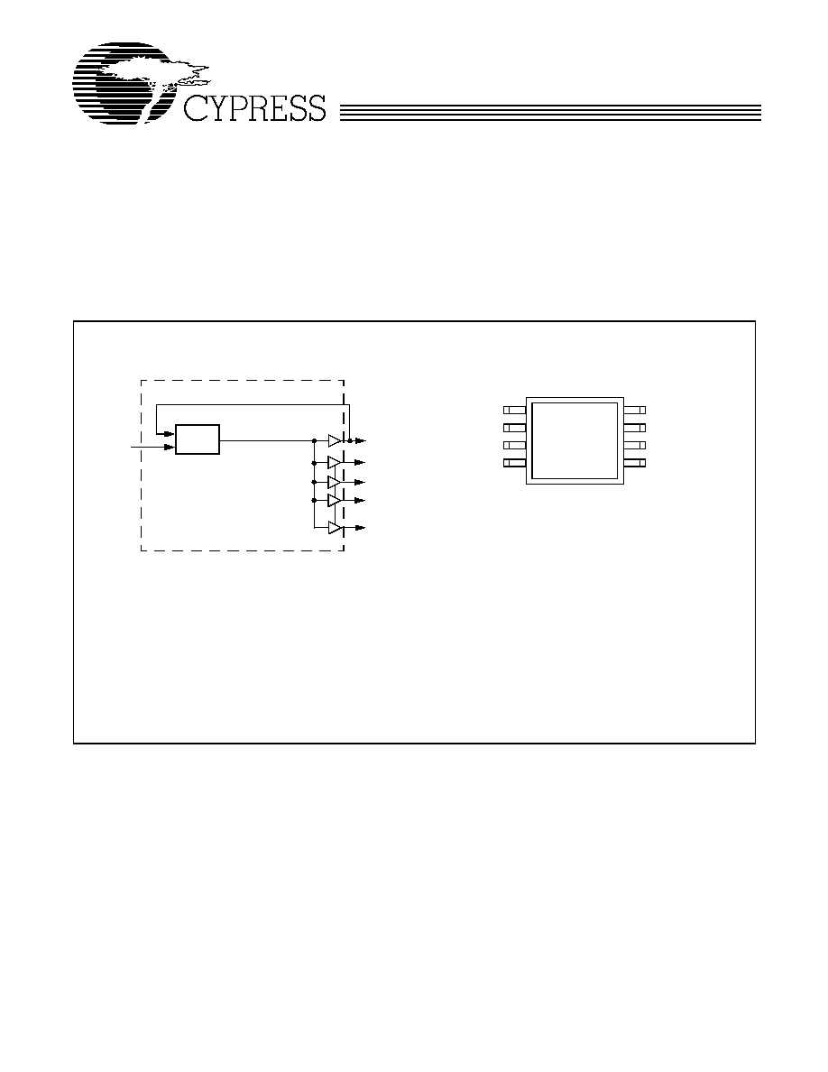
Block Diagram
Pin Configuration
Q0
PLL
REF
Q1
Q2
Q3
QFB
QFB
VDD
8
7
6
5
REF
Q0
Q1
GND
1
2
3
4
Q3
Q2
SOIC
W163
Document #: 38-07149 Rev. **
Page 2 of 5
Overview
The W163 products are five-output zero delay buffers. A
Phase-Locked Loop (PLL) is used to take a time-varying signal
and provide five copies of that same signal out. The internal
feedback to the PLL provides outputs in phase with the refer-
ence inputs.
Spread Aware
Many systems being designed now utilize a technology called
Spread Spectrum Frequency Timing Generation. Cypress has
been one of the pioneers of SSFTG development, and we de-
signed this product so as not to filter off the Spread Spectrum
feature of the Reference input, assuming it exists. When a
zero delay buffer is not designed to pass the SS feature
through, the result is a significant amount of tracking skew
which may cause problems in systems requiring synchroniza-
tion.
For more details on Spread Spectrum timing technology,
please see the Cypress Application note titled, "EMI Suppres-
sion Techniques with Spread Spectrum Frequency Timing
Generator (SSFTG) ICs."
Schematic
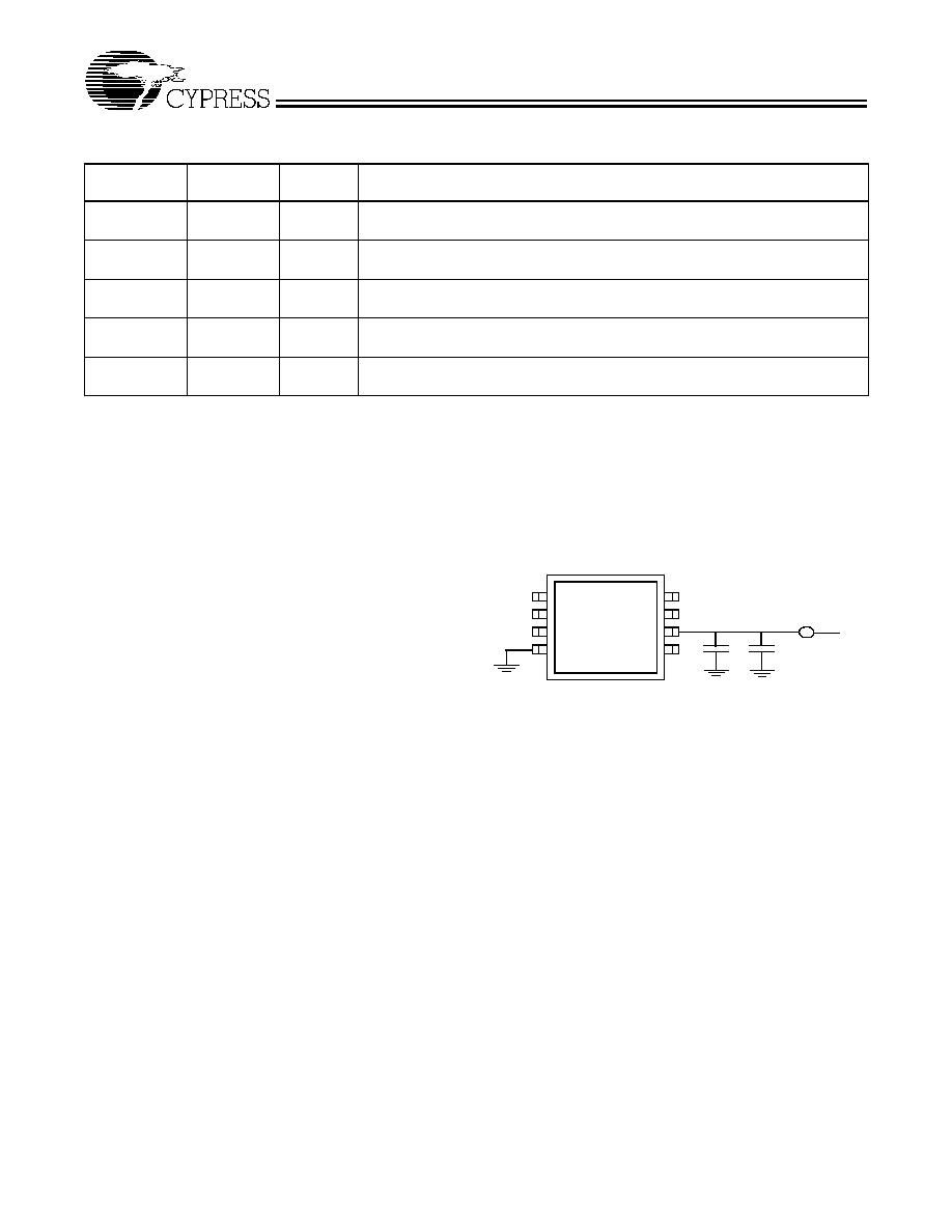
Pin Definitions
Pin Name
Pin No.
Pin
Type
Pin Description
REF
1
I
Reference Input: The output signals Q0:3 will be synchronized to this signal
unless the device is programmed to bypass the PLL.
Q0:3
2, 3, 5, 7
O
Outputs: These signals will be synchronous and of equal frequency to the signal
input at pin 1.
QFB
8
O
Feedback Output: This output signal does not vary from signals Q0:3 in function,
but is noted as the signal used to establish the propagation delay of nearly 0.
VDD
6
P
Power Connections: Connect to 3.3V. Use ferrite beads to help reduce noise
for optimal jitter performance.
GND
4
P
Ground Connections: Connect all grounds to the common system ground
plane.
Q0
Q1
GND
QFB
Q3
VDD
Q2
V
DD
Ferrite
Bead
10
µ
F
0.1
µ
F
REF
W163
Document #: 38-07149 Rev. **
Page 3 of 5
Absolute Maximum Ratings
Stresses greater than those listed in this table may cause per-
manent damage to the device. These represent a stress rating
only. Operation of the device at these or any other conditions
above those specified in the operating sections of this specifi-
cation is not implied. Maximum conditions for extended peri-
ods may affect reliability.
.
Parameter
Description
Rating
Unit
V
DD
, V
IN
Voltage on any pin with respect to GND
≠0.5 to +7.0
V
T
STG
Storage Temperature
≠65 to +150
∞C
T
A
Operating Temperature
0 to +70
∞C
T
B
Ambient Temperature under Bias
≠55 to +125
∞C
P
D
Power Dissipation
0.5
W
DC Electrical Characteristics
: T
A
=0∞C to 70∞C, V
DD
= 3.3V ±10%
Parameter
Description
Test Condition
Min
Typ
Max
Unit
I
DD
Supply Current
Unloaded, 100 MHz
40
mA
V
IL
Input Low Voltage
0.8
V
V
IH
Input High Voltage
2.0
V
V
OL
Output Low Voltage
I
OL
= 12 mA (-15)
I
OL
= 8 mA (-5)
0.4
V
V
OH
Output High Voltage
I
OL
= 12 mA (-15)
I
OL
= 8 mA (-5)
2.4
V
I
IL
Input Low Current
V
IN
= 0V
50
µ
A
I
IH
Input High Current
V
IN
= V
DD
100
µ
A
AC Electrical Characteristics:
T
A
= 0∞C to +70∞C, V
DD
= 3.3V ±10%
Parameter
Description
Test Condition
Min
Typ
Max
Unit
f
IN
Input Frequency
10
133
MHz
f
OUT
Output Frequency
15-pF load
[5]
10
133
MHz
t
R
Output Rise Time (-05)
[1]
2.0 to 0.8V, 15-pF load
2.5
ns
Output Rise Time (-15)
[1]
2.0 to 0.8V, 20-pF load
1.5
ns
t
F
Output Fall Time (-05)
[1]
2.0 to 0.8V, 15-pF load
2.5
ns
Output Rise Time (-15)
[1]
2.0 to 0.8V, 20-pF load
1.5
ns
t
ICLKR
Input Clock Rise Time
[1]
?
ns
t
ICLKF
Input Clock Fall Time
[1]
?
ns
t
PD
FBIN to REF Skew
[2, 3]
Measured at V
DD
/2
≠350
0
350
ps
t
SK
Output to Output Skew
All outputs loaded equally
≠250
0
250
ps
t
SKDD
Device to Device Skew
Measured at FBIN pins,
V
DD
/2
≠700
0
700
ps
t
D
Duty Cycle
15-pF load
[4]
45
50
55
%
t
LOCK
PLL Lock Time
Power supply stable and
1.0
ms
t
JC
Jitter, Cycle-to-Cycle
200
ps
Notes:
1.
Longer input rise and fall time will degrade skew and jitter performance.
2.
All AC specifications are measured with a 50
transmission line, load terminated with 50
to 1.4V.
3.
Skew is measured at 1.4V on rising edges.
4.
Duty cycle is measured at 1.4V.
5.
For the higher drive -15, the load is 20 pF.
W163
Document #: 38-07149 Rev. **
Page 4 of 5
© Cypress Semiconductor Corporation, 2001. The information contained herein is subject to change without notice. Cypress Semiconductor Corporation assumes no responsibility for the use
of any circuitry other than circuitry embodied in a Cypress Semiconductor product. Nor does it convey or imply any license under patent or other rights. Cypress Semiconductor does not authorize
its products for use as critical components in life-support systems where a malfunction or failure may reasonably be expected to result in significant injury to the user. The inclusion of Cypress
Semiconductor products in life-support systems application implies that the manufacturer assumes all risk of such use and in doing so indemnifies Cypress Semiconductor against all charges.
Ordering Information
Ordering Code
Option
Package
Name
Package Type
W163
-05, -15
G
8-pin Plastic SOIC (150-mil)
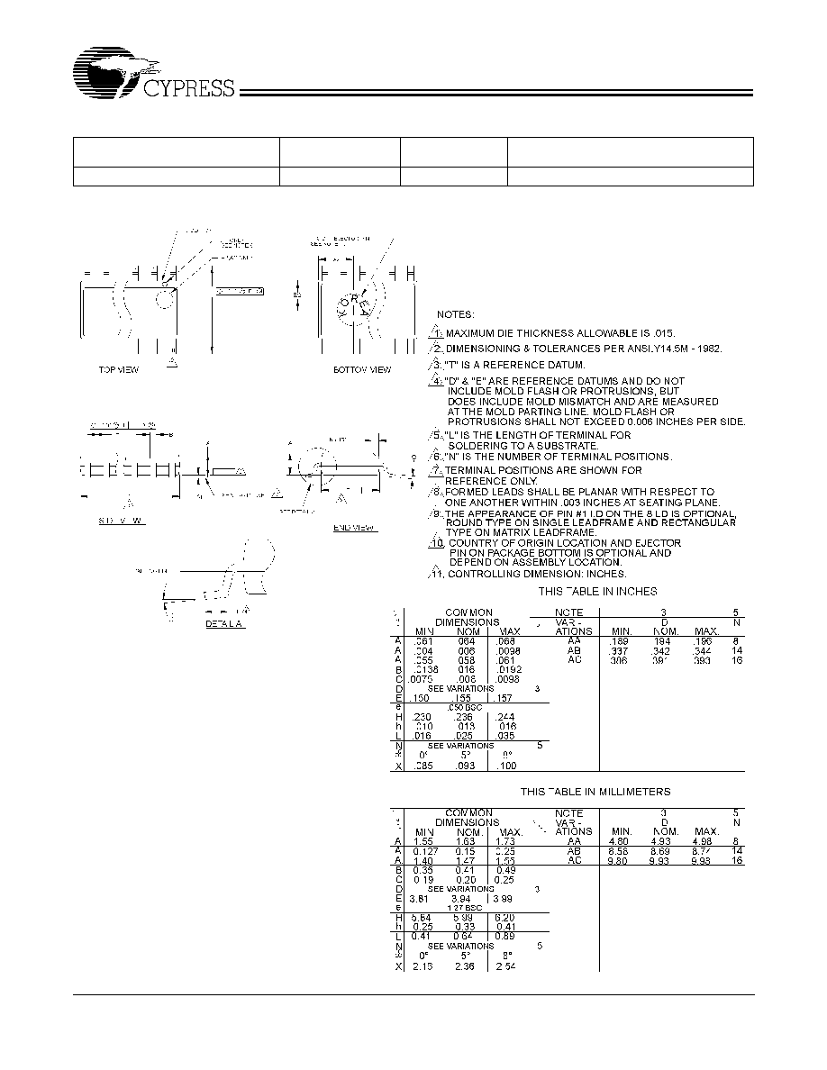
Package Diagram
8-Pin Small Outline Integrated Circuit (SOIC, 150-mil)

W163
Document #: 38-07149 Rev. **
Page 5 of 5
Document Title: W163 Spread AwareTM, Zero Delay Buffer
Document Number: 38-07149
REV.
ECN NO.
Issue
Date
Orig. of
Change
Description of Change
**
110258
12/15/01
SZV
Change from Spec number: 38-00787 to 38-07149