 | –≠–ª–µ–∫—Ç—Ä–æ–Ω–Ω—ã–π –∫–æ–º–ø–æ–Ω–µ–Ω—Ç: W166 | –°–∫–∞—á–∞—Ç—å:  PDF PDF  ZIP ZIP |
Spread Spectrum Frequency Timing Generator
W166
Cypress Semiconductor Corporation
∑
3901 North First Street
∑
San Jose
∑
CA 95134
∑
408-943-2600
December 20, 1999, rev. **
Features
∑ Maximized EMI suppression using Cypress's Spread
Spectrum technology
∑ Generates a spread spectrum copy of the provided
input
∑ Selectable spreading characteristics
∑ Integrated loop filter components
∑ Operates with a 3.3V or 5V supply
∑ SSON# pin enables frequency spreading
∑ Low power CMOS design
∑ Available in 8-pin SOIC (Small Outline Integrated
Circuit)
Overview
The W166 incorporates the latest advances in PLL spread
spectrum frequency synthesizer techniques. By frequency
modulating the output with a low-frequency carrier, peak EMI
is greatly reduced. Use of this technology allows systems to
pass increasingly difficult EMI testing without resorting to cost-
ly shielding or redesign.
In a system, not only is EMI reduced in the various clock lines,
but also in all signals which are synchronized to the clock.
Therefore, the benefits of using this technology increase with
the number of address and data lines in the system. The Sim-
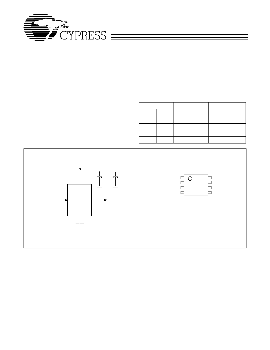
plified Block Diagram shows a simple implementation.
Table 1. Frequency Spread Selection
W166
Input
Frequency
(MHz)
Output
Frequency (MHz)
FS1
FS0
0
0
50 to 65
f
IN
±0.625%
0
1
50 to 65
f
IN
±1.25%
1
0
50 to 65
f
IN
±2.5%
1
1
50 to 65
f
IN
≠3.75%
Simplified Block Diagram
Pin Configuration
Oscillator or Reference
Spread Spectrum
W166
(EMI suppressed)
3.3V or 5V
Input
Output
W1
6
6
8
7
6
5
1
2
3
4
CLKIN
NC
GND
FS1
SSON#
CLKOUT
FS0
VDD

W166
2
Functional Description
The W166 uses a Phase-Locked Loop (PLL) to frequency
modulate an input clock. The result is an output clock whose
frequency is slowly swept over a narrow band near the input
signal. The basic circuit topology is shown in Figure 1. The
input reference signal is divided by Q and fed to the phase
detector. A signal from the VCO is divided by P and fed back
to the phase detector also. The PLL will force the frequency of
the VCO output signal to change until the divided output signal
and the divided reference signal match at the phase detector
input. The output frequency is then equal to the ratio of P/Q
times the reference frequency. (Note: For the W166 the output
frequency is equal to the input frequency.) The unique feature
of the Spread Spectrum Frequency Timing Generator is that a
modulating waveform is superimposed at the input to the VCO.
This causes the VCO output to be slowly swept across a pre-
determined frequency band.
Because the modulating frequency is typically 1000 times
slower than the fundamental clock, the spread spectrum pro-
cess has little impact on system performance.
Frequency Selection With SSFTG
In Spread Spectrum Frequency Timing Generation, EMI re-
duction depends on the shape, modulation percentage, and
frequency of the modulating waveform. While the shape and
frequency of the modulating waveform are fixed, the modula-
tion percentage may be varied.
A larger spreading percentage improves EMI reduction. How-
ever, large spread percentages may either exceed system
maximum frequency ratings or lower the average frequency to
a point where performance is affected. For these reasons, nar-
row and wide modulation selections are provided.
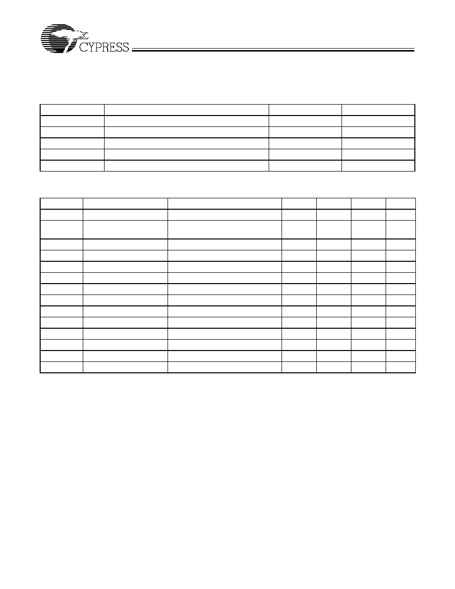
Pin Definitions
Pin Name
Pin No.
Pin
Type
Pin Description
CLKOUT
7
O
Output Modulated Frequency: Frequency modulated copy of the reference input
(SSON# asserted).
CLKIN
1
I
External Reference Frequency Input: Clock input.
NC
2
NC
No Connect: This pin must be left unconnected.
SSON#
8
I
Spread Spectrum Control (Active LOW): Asserting this signal (active LOW) turns the
internal modulation waveform on. This pin has an internal pull-down resistor.
FS0:1
6, 4
I
Frequency Selection Bits 0,1: These pins select the frequency spreading characteris-
tics. Refer to Table 1. These pins have internal pull-up resistors.
VDD
5
P
Power Connection: Connected to 3.3V or 5V power supply.
GND
3
G
Ground Connection: This should be connected to the common ground plane.
Freq.
Phase
Modulating
VCO
Post
CLKOUT
Detector
Charge
Pump
Waveform
Dividers
Divider
Feedback
Divider
PLL
GND
VDD
Q
P
Clock Input
Reference Input
(EMI suppressed)
Figure 1. System Block Diagram

W166
3
Spread Spectrum Frequency Timing Generator
The device generates a clock that is frequency modulated in
order to increase the bandwidth that it occupies. By increasing
the bandwidth of the fundamental and its harmonics, the am-
plitudes of the radiated electromagnetic emissions are re-
duced. This effect is depicted in Figure 2.
As shown in Figure 2, a harmonic of a modulated clock has a
much lower amplitude than that of an unmodulated signal. The
reduction in amplitude is dependent on the harmonic number
and the frequency deviation or spread. The equation for the
reduction is
dB = 6.5 + 9*log
10
(P) + 9*log
10
(F)
Where P is the percentage of deviation and F is the frequency
in MHz where the reduction is measured.
The output clock is modulated with a waveform depicted in
Figure 3. This waveform, as discussed in "Spread Spectrum
Clock Generation for the Reduction of Radiated Emissions" by
Bush, Fessler, and Hardin produces the maximum reduction
in the amplitude of radiated electromagnetic emissions. The
deviation selected for this chip is ±0.45% or 0.6% of the select-
ed frequency. Figure 3 details the Cypress spreading pattern.
Cypress does offer options with more spread and greater EMI
reduction. Contact your local Sales representative for details
on these devices.
S SFTG
Typical Clock
Frequency Span (MHz)
A
m
p
lit
u
d
e
(
d
B
)
S p re a d
S p e ctru m
E n a b le d
E M I R e d u ctio n
S p re a d
Spectrum
N o n -
Frequency Span (MHz)
Down Spread
Am
p
l
i
t
u
d
e
(
d
B)
C enter Sp read
Figure 2. Clock Harmonic with and without SSCG Modulation Frequency Domain Representation
MAX.
MIN.
10
%
20
%
30
%
40
%
50
%
60
%
70
%
80
%
90
%
10
0%
10
%
20
%
30
%
40
%
50
%
60
%
70
%
80
%
90
%
10
0%
F
R
E
Q
UENCY
Figure 3. Typical Modulation Profile
W166
4
Absolute Maximum Ratings
Stresses greater than those listed in this table may cause per-
manent damage to the device. These represent a stress rating
only. Operation of the device at these or any other conditions
above those specified in the operating sections of this specifi-
cation is not implied. Maximum conditions for extended peri-
ods may affect reliability
.
Parameter
Description
Rating
Unit
V
DD
, V
IN
Voltage on any Pin with Respect to GND
≠0.5 to +7.0
V
T
STG
Storage Temperature
≠65 to +150
∞C
T
A
Operating Temperature
0 to +70
∞C
T
B
Ambient Temperature under Bias
≠55 to +125
∞C
P
D
Power Dissipation
0.5
W
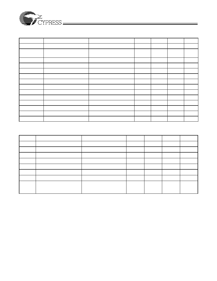
DC Electrical Characteristics
: 0∞C < T
A
< 70∞C, V
DD
= 3.3V ±5%
Parameter
Description
Test Condition
Min
Typ
Max
Unit
I
DD
Supply Current
18
32
mA
t
ON
Power Up Time
First locked clock cycle after Power
Good
5
ms
V
IL
Input Low Voltage
0.8
V
V
IH
Input High Voltage
2.4
V
V
OL
Output Low Voltage
0.4
V
V
OH
Output High Voltage
2.4
V
I
IL
Input Low Current
Note 1
≠20
µ
A
I
IH
Input High Current
Note 1
20
µ
A
I
OL
Output Low Current
@ 0.4V, V
DD
= 3.3V
15
mA
I
OH
Output High Current
@ 2.4V, V
DD
= 3.3V
15
mA
C
I
Input Capacitance
All pins except CLKIN
7
pF
C
I
Input Capacitance
CLKIN pin only
6
5
pF
R
P
Input Pull-Up Resistor
500
k
Z
OUT
Clock Output Impedance
25
Note:
1.
Inputs FS1:0 have a pull-up resistor, Input SSON# has a pull-down resistor.
W166
5
DC Electrical Characteristics:
0∞C < T
A
< 70∞C, V
DD
= 5V ±10%
Parameter
Description
Test Condition
Min
Typ
Max
Unit
I
DD
Supply Current
21
40
mA
t
ON
Power Up Time
First locked clock cycle after
Power Good
5
ms
V
IL
Input Low Voltage
0.8
V
V
IH
Input High Voltage
3.5
V
V
OL
Output Low Voltage
0.4
V
V
OH
Output High Voltage
2.4
V
I
IL
Input Low Current
Note 1
≠20
µ
A
I
IH
Input High Current
Note 1
20
µ
A
I
OL
Output Low Current
@ 0.4V, V
DD
= 5V
24
mA
I
OH
Output High Current
@ 2.4V, V
DD
= 5V
24
mA
C
I
Input Capacitance
All pins except CLKIN
7
pF
C
I
Input Capacitance
CLKIN pin only
5
pF
R
P
Input Pull-Up Resistor
500
k
Z
OUT
Clock Output Impedance
25
AC Electrical Characteristics:
T
A
= 0∞C to +70∞C, V
DD
= 3.3V ±5% or 5V±10%
Symbol
Parameter
Test Condition
Min
Typ
Max
Unit
f
IN
Input Frequency
Input Clock
50
65
MHz
f
OUT
Output Frequency
Spread Off
50
65
MHz
t
R
Output Rise Time
15-pF load, 0.8V≠2.4V
2
5
ns
t
F
Output Fall Time
15-pF load, 2.4V≠0.8V
2
5
ns
t
OD
Output Duty Cycle
15-pF load, test at V
DD
/2
40
60
%
t
ID
Input Duty Cycle
40
60
%
t
JCYC
Jitter, Cycle-to-Cycle
250
300
ps
Harmonic Reduction
f
out
= 50 MHz, third harmonic
measured, reference board,
15-pF load
8
dB