 | –≠–ª–µ–∫—Ç—Ä–æ–Ω–Ω—ã–π –∫–æ–º–ø–æ–Ω–µ–Ω—Ç: W170 | –°–∫–∞—á–∞—Ç—å:  PDF PDF  ZIP ZIP |
Spread AwareTM, Frequency Multiplier and Zero Delay Buffer
W170-01
Cypress Semiconductor Corporation
∑
3901 North First Street
∑
San Jose
∑
CA 95134
∑
408-943-2600
September 28, 1999, rev. **
Features
∑ Spread AwareTM--designed to work with SSFTG
reference signals
∑ Two outputs
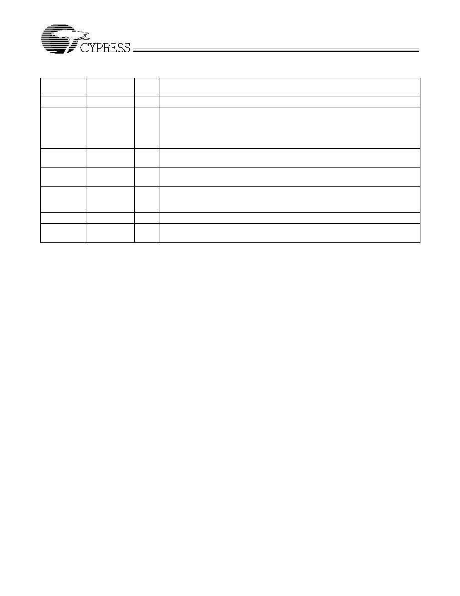
∑ Configuration options allow various multiplication of
the reference frequency, refer to Table 1 to determine
the specific option which meets your multiplication
needs
∑ Available in 8-pin SOIC package
Key Specifications
Operating Voltage: ...........................3.3V±5% or 5.0V± 10%
Operating Range: .......................20 MHz < f
OUT1
< 133 MHz
Absolute Jitter: ......................................................... ±500 ps
Output to Output Skew: .............................................. 250 ps
Propagation Delay: ................................................... ±350 ps
Propagation delay is affected by input rise time.
Table 1. Configuration Options
FBIN
FS0
FS1
OUT1
OUT2
OUT1
0
0
2 X REF
REF
OUT1
1
0
4 X REF
2 X REF
OUT1
0
1
REF
REF/2
OUT1
1
1
8 X REF
4 X REF
OUT2
0
0
4 X REF
2 X REF
OUT2
1
0
8 X REF
4 X REF
OUT2
0
1
2 X REF
REF
OUT2
1
1
16 X REF
8 X REF
Spread Aware is a trademark of Cypress Semiconductor Corporation.
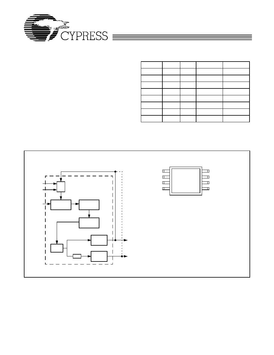
Block Diagram
Pin Configuration
˜Q
FS0
FS1
Reference
FBIN
Phase
Detector
Charge
Pump
Loop
Filter
VCO
˜2
Output
Buffer
OUT1
OUT2
Output
Buffer
External feedback connection to
OUT1 or OUT2, not both
Input
IN
OUT2
VDD
OUT1
FS1
8
7
6
5
FBIN
IN
GND
FS0
1
2
3
4
W170-01
2
Overview
The W170-01 is a two-output zero delay buffer and frequency
multiplier. It provides an external feedback path allowing max-
imum flexibility when implementing the Zero Delay feature.
This is explained further in the sections of this data sheet titled
"How to Implement Zero Delay," and "Inserting Other Devices
in Feedback Path."
The W170-01 is a pin-compatible upgrade of the Cypress
W42C70-01. The W170-01 addresses some application de-
pendent problems experienced by users of the older device.
Most importantly, it addresses the tracking skew problem in-
duced by a reference which has Spread Spectrum Timing en-
abled on it.
Spread Aware
Many systems being designed now utilize a technology called
Spread Spectrum Frequency Timing Generation. Cypress has
been one of the pioneers of SSFTG development, and we de-
signed this product so as not to filter off the Spread Spectrum
feature of the Reference input, assuming it exists. When a zero
delay buffer is not designed to pass the SS feature through,
the result is a significant amount of tracking skew which may
cause problems in systems requiring synchronization.
For more details on Spread Spectrum timing technology,
please see the Cypress application note titled, "EMI Suppres-
sion Techniques with Spread Spectrum Frequency Timing
Generator (SSFTG) ICs."
Pin Definitions
Pin Name
Pin No.
Pin
Type
Pin Description
IN
2
I
Reference Input: The output signals will be synchronized to this signal.
FBIN
1
I
Feedback Input: This input must be fed by one of the outputs (OUT1 or OUT2) to
ensure proper functionality. If the trace between FBIN and the output pin being used
for feedback is equal in length to the traces between the outputs and the signal desti-
nations, then the signals received at the destinations will be synchronized to the REF
signal input (IN).
OUT1
6
O
Output 1: The frequency of the signal provided by this pin is determined by the feed-
back signal connected to FBIN, and the FS0:1 inputs (see Table 1).
OUT2
8
O
Output 2: The frequency of the signal provided by this pin is one-half of the frequency
of OUT1. See Table 1.
VDD
7
P
Power Connections: Connect to 3.3V or 5V. This pin should be bypassed with a
0.1-
µ
F decoupling capacitor. Use ferrite beads to help reduce noise for optimal jitter
performance.
GND
3
P
Ground Connection: Connect all grounds to the common system ground plane.
FS0:1
4, 5
I
Function Select Inputs: Tie to VDD (HIGH, 1) or GND (LOW, 0) as desired per
Table 1.
W170-01
3
How to Implement Zero Delay
Typically, zero delay buffers (ZDBs) are used because a de-
signer wants to provide multiple copies of a clock signal in
phase with each other. The whole concept behind ZDBs is that
the signals at the destination chips are all going HIGH at the
same time as the input to the ZDB. In order to achieve this,
layout must compensate for trace length between the ZDB and
the target devices. The method of compensation is described
below.
External feedback is the trait that allows for this compensation.
The PLL on the ZDB will cause the feedback signal to be in
phase with the reference signal. When laying out the board,
match the trace lengths between the output being used for
feed back and the FBIN input to the PLL.
If it is desirable to either add a little delay, or slightly precede
the input signal, this may also be affected by either making the
trace to the FBIN pin a little shorter or a little longer than the
traces to the devices being clocked.
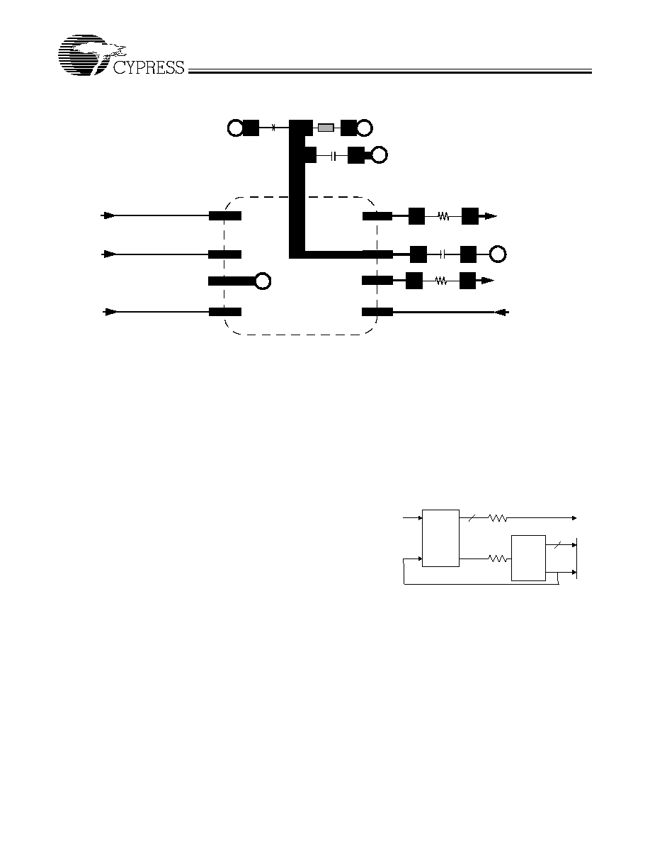
Inserting Other Devices in Feedback Path
Another nice feature available due to the external feedback is
the ability to synchronize signals up to the signal coming from
some other device. This implementation can be applied to any
device (ASIC, multiple output clock buffer/driver, etc.) which is
put into the feedback path.
Referring to Figure 2, if the traces between the ASIC/Buffer
and the destination of the clock signal(s) (A) are equal in length
to the trace between the buffer and the FBIN pin, the signals
at the destination(s) device will be driven HIGH at the same
time the Reference clock provided to the ZDB goes HIGH.
Synchronizing the other outputs of the ZDB to the outputs from
the ASIC/Buffer is more complex however, as any propagation
delay in the ASIC/Buffer must be accounted for.
Figure 1. Schematic/Suggested Layout
C8
G
Ferrite
Bead
Power Supply Connection
V+
G
C
A
G
FS1
FS0
GND
IN
FBIN
10 µF
0.01 µF
1
2
3
4
8
7
6
5
22
22
G
C9 = 0.1 µF
OUTPUT 1
OUTPUT 2
OUT 2
V
DD
OUT 1
Reference
Signal
Feedback
Input
ASIC/
Buffer
Zero
Delay
Buffer
A
Figure 2. 6 Output Buffer in the Feedback Path
W170-01
4
Absolute Maximum Ratings
Stresses greater than those listed in this table may cause per-
manent damage to the device. These represent a stress rating
only. Operation of the device at these or any other conditions
above those specified in the operating sections of this specifi-
cation is not implied. Maximum conditions for extended peri-
ods may affect reliability.
.
Parameter
Description
Rating
Unit
V
DD
, V
IN
Voltage on any pin with respect to GND
≠0.5 to +7.0
V
T
STG
Storage Temperature
≠65 to +150
∞C
T
A
Operating Temperature
0 to +70
∞C
T
B
Ambient Temperature under Bias
≠55 to +125
∞C
P
D
Power Dissipation
0.5
W
DC Electrical Characteristics
: T
A
=0∞C to 70∞C, V
DD
= 3.3V ±5%
Parameter
Description
Test Condition
Min
Typ
Max
Unit
I
DD
Supply Current
Unloaded, 133 MHz
17
35
mA
V
IL
Input Low Voltage
0.8
V
V
IH
Input High Voltage
2.0
V
V
OL
Output Low Voltage
I
OL
= 8 mA
0.4
V
V
OH
Output High Voltage
I
OH
= 8 mA
2.4
V
I
IL
Input Low Current
V
IN
= 0V
5
µ
A
I
IH
Input High Current
V
IN
= V
DD
5
µ
A
DC Electrical Characteristics
: T
A
=0∞C to 70∞C, V
DD
= 5V ±10%
Parameter
Description
Test Condition
Min
Typ
Max
Unit
I
DD
Supply Current
Unloaded, 133 MHz
31
50
mA
V
IL
Input Low Voltage
0.8
V
V
IH
Input High Voltage
2.0
V
V
OL
Output Low Voltage
I
OL
= 8 mA
0.4
V
V
OH
Output High Voltage
I
OH
= 8 mA
2.4
V
I
IL
Input Low Current
V
IN
= 0V
5
µ
A
I
IH
Input High Current
V
IN
= V
DD
5
µ
A
W170-01
5
Document #: 38-00795
AC Electrical Characteristics:
T
A
= 0∞C to +70∞C, V
DD
= 3.3V±5%
Parameter
Description
Test Condition
Min
Typ
Max
Unit
f
IN
Input Frequency
[1]
OUT2 = REF
MHz
f
OUT
Output Frequency
OUT1
20
133
MHz
t
R
Output Rise Time
0.8V to 2.0V, 15-pF load
3.5
ns
t
F
Output Fall Time
2.0V to 0.8V, 15-pF load
2.5
ns
t
ICLKR
Input Clock Rise Time
[2]
10
ns
t
ICLKF
Input Clock Fall Time
[2]
10
ns
t
PD
FBIN to IN (Reference Input) Skew
[3, 4]
Note 4
300
ps
t
D
Duty Cycle
Note 5
40
50
60
%
t
LOCK
PLL Lock Time
Power supply stable
1.0
ms
t
JC
Jitter, Cycle-to-Cycle
Note 6
200
ps
AC Electrical Characteristics:
T
A
= 0∞C to +70∞C, V
DD
= 5V±10%
Parameter
Description
Test Condition
Min
Typ
Max
Unit
f
IN
Input Frequency
[1]
OUT2 = REF
MHz
f
OUT
Output Frequency
OUT1
20
133
MHz
t
R
Output Rise Time
0.8V to 2.0V, 15-pF load
3.5
ns
t
F
Output Fall Time
2.0V to 0.8V, 15-pF load
2.5
ns
t
ICLKR
Input Clock Rise Time
[2]
10
ns
t
ICLKF
Input Clock Fall Time
[2]
10
ns
t
PD
FBIN to IN (Reference Input) Skew
[3, 4]
Note 4
300
ps
t
D
Duty Cycle
Note 7, 8
40
50
60
%
t
LOCK
PLL Lock Time
Power supply stable
1.0
ms
t
JC
Jitter, Cycle-to-Cycle
Note 6
200
ps
Notes:
1.
Input frequency is limited by output frequency range and input to output frequency multiplication factor (which is determined by circuit configuration).
2.
Longer input rise and fall time will degrade skew and jitter performance.
3.
All AC specifications are measured with a 50
transmission line, load terminated with 50
to 1.4V.
4.
Skew is measured at 1.4V on rising edges.
5.
Duty cycle is measured at 1.4V.
6.
Jitter is measured on 133-MHz signal at 1.4V.
7.
Duty cycle is measured at 1.4V, 120 MHz.
8.
Duty cycle at 133 MHz is 35/65 worst case.
Ordering Information
Ordering Code
Option
Package
Name
Package Type
W170
-01
G
8-pin SOIC (150 mil)