 | –≠–ª–µ–∫—Ç—Ä–æ–Ω–Ω—ã–π –∫–æ–º–ø–æ–Ω–µ–Ω—Ç: W191H | –°–∫–∞—á–∞—Ç—å:  PDF PDF  ZIP ZIP |
Skew Controlled SDRAM Buffer
W191
Cypress Semiconductor Corporation
∑
3901 North First Street
∑
San Jose
∑
CA 95134
∑
408-943-2600
Document #: 38-07008 Rev. *B
Revised December 17, 2002
Features
∑ Six skew controlled CMOS outputs
∑ Output skew between any two outputs is less than
150 ps
∑ SMBus Serial configuration interface
∑ 2.5 ns to 5 ns propagation delay
∑ DC to 133 MHz operation (Commercial)
∑ DC to 100 MHz operation (Industrial)
∑ Single 3.3V supply voltage
∑ Low power CMOS design packaged in a 16-pin SSOP
(Small Shrink Outline Package)
Key Specifications
Supply Voltages:...................................... V
DDQ3
= 3.3V ±5%
Operating Temperature: (Commercial) ............. 0∞C to +70∞C
Operating Temperature: (Industrial) ............. ≠40∞C to +85∞C
Input Threshold: .................................................. 1.5V typical
Maximum Input Voltage: ...................................V
DDQ3
+ 0.5V
Input Frequency: (Commercial) ........................ 0 to 133 MHz
Input Frequency: (Industrial) ............................ 0 to 100 MHz
BUF_IN to SDRAM0:5 Propagation Delay: ...... 2.5 ns to 5 ns
Min. Output Edge Rate: ............................................. 1.0V/ns
Max. Output Skew: ...................................................... 150 ps
Output Duty Cycle: .................................. 45/55% worst case
Output Impedance: ................................................... 15
typ.
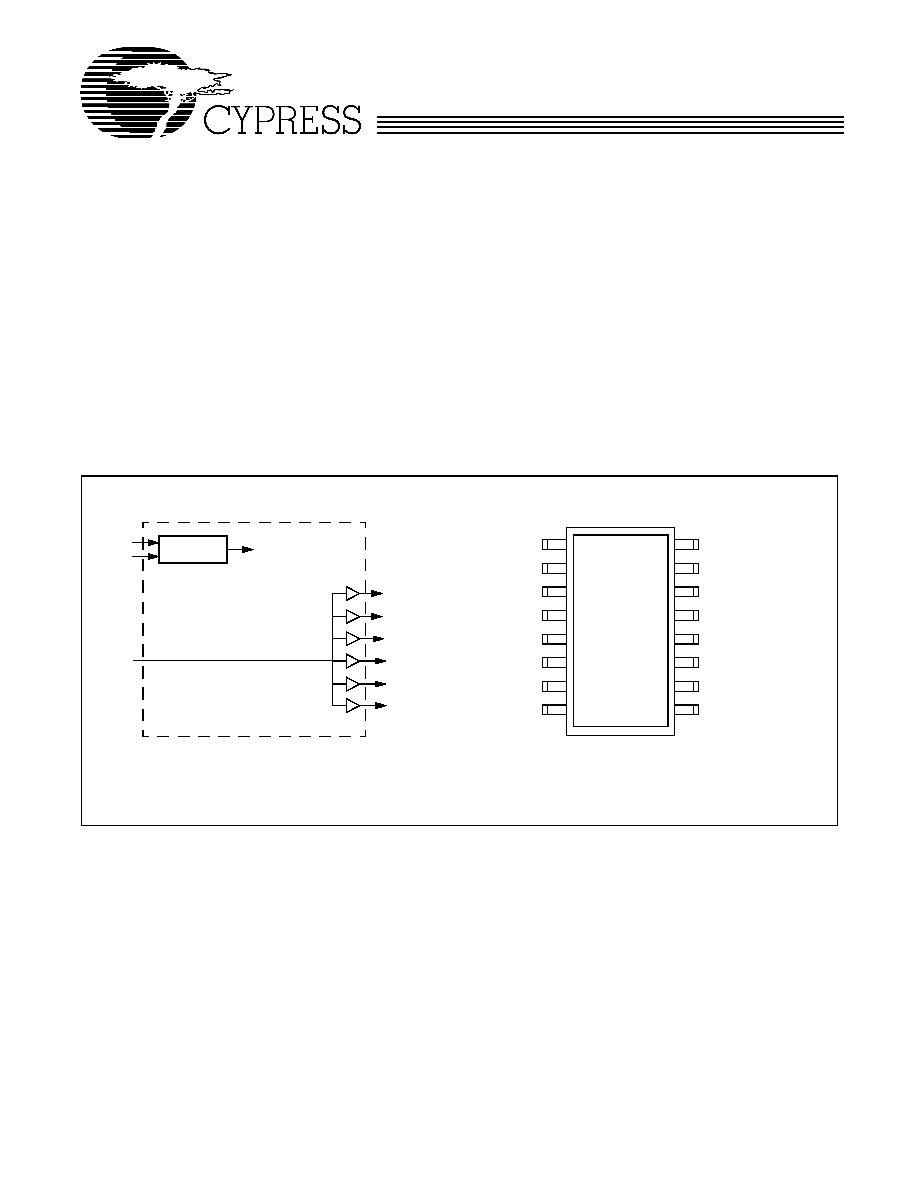
Block Diagram
Pin Configuration
[1]
SDRAM0
SDRAM1
SDRAM2
SDRAM3
SDRAM4
SDRAM5
SMBus
SCLOCK
SDATA
Device Control
BUF_IN
VDDQ3
SDRAM5
GND
SDRAM4
VDDQ3
SDRAM3
GND
SCLK
16
15
14
13
12
11
10
9
SDRAM0
GND
SDRAM1
BUF_IN
GND
SDRAM2
VDDQ3
SDATA
1
2
3
4
5
6
7
8
Note:
1.
Internal pull-up resistor of 250K on SDATA and SCLK.
W191
Document #: 38-07008 Rev. *B
Page 2 of 10
Overview
The W191 is a skew controlled fanout buffer optimized for
interface with registered DIMMs.
Functional Description
Output Drivers
The W191 output buffers are CMOS type which deliver a
rail-to-rail (GND to VDD) output voltage swing into a nominal
capacitive load. Thus, output signaling is both TTL and CMOS
level compatible. Nominal output buffer impedance is 15
.
Serial Control
Serial control data is written to the W191 in ten bytes of eight
bits each. Bytes are written in the order shown in Table 1
Writing Data Bytes
Each bit in the data bytes control a particular device function.
Bits are written MSB (most significant bit) first, which is bit 7.
Table 1 gives the bit formats for registers located in Data
Bytes 0-2.
Pin Definitions
Pin Name
Pin No.
Pin
Type
Pin Description
SDRAM0:5
1, 3, 6,
11, 13, 15
O
SDRAM Outputs: Provides buffered copy of BUF_IN. The propagation delay from a
rising input edge to a rising output edge is 2.5 to 5 ns. All outputs are skew controlled
to within ±150 ps of each other.
BUF_IN
4
I
Clock Input: This clock input has an input threshold voltage of 1.5V (typ).
SDATA
8
I/O
SMBus Data input: Data should be presented to this input as described in the SMBus
section of this data sheet. Internal 250-k
pull-up resistor.
SCLOCK
9
I
SMBus clock input: The SMBus Data clock should be presented to this input as
described in the SMBus section of this data sheet. Internal 250-k
pull-up resistor.
VDDQ3
7, 12, 16
P
Power Connection: Power supply for core logic and output buffers. Connected to 3.3V
supply.
GND
2, 5, 10,
14
G
Ground Connection: Connect all ground pins to the common system ground plane.
Table 1. Byte Writing Sequence
Byte
Sequence
Byte Name
Bit Sequence
Byte Description
1
Slave Address
11010010
Commands the W191 to accept the bits in Data Bytes 0-6 for internal
register configuration. Since other devices may exist on the same com-
mon serial data bus, it is necessary to have a specific slave address for
each potential receiver. The slave receiver address for the W191 is
11010010. Register setting will not be made if the Slave Address is not
correct (or is for an alternate slave receiver).
2
Command Code
Don't Care
Unused by the W191, therefore bit values are ignored (don't care). This
byte must be included in the data write sequence to maintain proper byte
allocation. The Command Code Byte is part of the standard serial com-
munication protocol and may be used when writing to another addressed
slave receiver on the serial data bus.
3
Byte Count
Don't Care
Unused by the W191, therefore bit values are ignored (don't care). This
byte must be included in the data write sequence to maintain proper byte
allocation. The Byte Count Byte is part of the standard serial communi-
cation protocol and may be used when writing to another addressed slave
receiver on the serial data bus.
4
Data Byte 0
Refer to
Table 2
The data bits in these bytes set internal W191 registers that control device
operation. The data bits are only accepted when the Address Byte bit
sequence is 11010010, as noted above. For description of bit control
functions, refer to Table 2.
5
Data Byte 1
6
Data Byte 2
7
Data Byte 3
Don't Care
8
Data Byte 4
9
Data Byte 5
10
Data Byte 6

W191
Document #: 38-07008 Rev. *B
Page 3 of 10
Table 2. Data Bytes 0≠2 Serial Configuration Map
[2]
Bit(s)
Affected Pin
Control Function
Bit Control
Pin No.
Pin Name
0
1
Data Byte 0 SDRAM Active/Inactive Register (1 = Enable, 0 = Disable)
7
6
SDRAM2
Clock Output Disable
Low
Active
6
--
--
(Reserved)
--
--
5
--
--
(Reserved)
--
--
4
--
--
(Reserved)
--
--
3
--
--
(Reserved)
--
--
2
3
SDRAM1
Clock Output Disable
Low
Active
1
--
--
(Reserved)
--
--
0
1
SDRAM0
Clock Output Disable
--
--
Data Byte 1 SDRAM Active/Inactive Register (1 = Enable, 0 = Disable)
7
--
--
Clock Output Disable
--
--
6
15
SDRAM5
Clock Output Disable
Low
Active
5
--
--
Clock Output Disable
--
--
4
--
--
(Reserved)
--
--
3
13
SDRAM4
Clock Output Disable
Low
Active
2
--
--
(Reserved)
--
--
1
--
--
(Reserved)
--
--
0
--
--
(Reserved)
--
--
Data Byte 2 SDRAM Active/Inactive Register (1 = Enable, 0 = Disable)
7
11
SDRAM3
Clock Output Disable
Low
Active
6
--
--
(Reserved)
--
--
5
--
--
(Reserved)
--
--
4
--
--
(Reserved)
--
--
3
--
--
(Reserved)
--
--
2
--
--
(Reserved)
--
--
1
--
--
(Reserved)
--
--
0
--
--
(Reserved)
--
--
Note:
2.
At power up all SDRAM outputs are enabled and active. Program Reserved bits to 0.
W191
Document #: 38-07008 Rev. *B
Page 4 of 10
Absolute Maximum Ratings
[3]
Stresses greater than those listed in this table may cause per-
manent damage to the device. These represent a stress rating
only. Operation of the device at these or any other conditions
above those specified in the operating sections of this specifi-
cation is not implied. Maximum conditions for extended peri-
ods may affect reliability.
DC Electrical Characteristics:
T
A
= 0∞C to +70∞C (Commercial), V
DDQ3
= 3.3V ± 5%,T
A
= -40∞C to +85∞C (Industrial),
V
DDQ3
= 3.3V ± 5%
[4]
Parameter
Description
Rating
Unit
V
DDQ3
, V
IN
Voltage on any pin with respect to GND
≠0.5 to + 7.0
V
T
STG
Storage Temperature
≠65 to + 150
∞C
T
B
Ambient Temperature under Bias
≠55 to + 125
∞C
T
A
Operating Temperature (Commercial)
0 to + 70
∞C
T
A
Operating Temperature (Industrial)
-40 to + 85
∞C
Parame-
ter
Description
Test Condition
Min.
Typ.
Max.
Unit
I
DD
3.3V Supply Current
BUF_IN = 100 MHz
173
mA
I
DD
3.3V Supply Current in three-state
BUF_IN = 100 MHz
5
mA
Logic Inputs (BUF_IN, OE, SCLOCK, SDATA)
V
IL
Input Low Voltage
GND≠0.3
0.8
V
V
IH
Input High Voltage
2.0
V
DDQ3
+0.5
V
I
ILEAK
Input Leakage Current, BUF_IN
≠5
+5
µA
I
ILEAK
Input Leakage Current
[5]
≠20
+5
µA
Logic Outputs (SDRAM0:5)
V
OL
Output Low Voltage
I
OL
= 1 mA
50
mV
V
OH
Output High Voltage
I
OH
= ≠1 mA
3.1
V
I
OL
Output Low Current
V
OL
= 1.5V
65
100
160
mA
I
OH
Output High Current
V
OH
= 1.5V
70
110
185
mA
Pin Capacitance/Inductance
C
IN
Input Pin Capacitance (Except BUF_IN)
5
pF
C
OUT
Output Pin Capacitance
6
pF
L
IN
Input Pin Inductance
7
nH
Notes:
3.
Multiple supplies: The voltage on any input or I/O pin cannot exceed the power pin during power-up. Power supply sequencing is NOT required.
4.
Outputs loaded by 6" 60
transmission lines with 20 pF capacitors.
5.
OE, SCLOCK, and SDATA logic pins have a 250-k
internal pull-up resistor (not CMOS level).
W191
Document #: 38-07008 Rev. *B
Page 5 of 10
AC Electrical Characteristics:
T
A
= 0∞C to +70∞C (Commercial), V
DDQ3
= 3.3V ± 5%,T
A
= -40∞C to +85∞C (Industrial),
V
DDQ3
= 3.3V ± 5% (Lump Capacitance Test Load = 30pF)
Parameter
Description
Test Condition
Min.
Typ.
Max.
Unit
f
IN
Input Frequency (Commercial)
0
133
MHz
f
IN
Input Frequency (Industrial)
0
100
MHz
t
R
Output Rise Edge Rate
Measured from 0.4V
to 2.4V
1.0
4.0
V/ns
t
F
Output Fall Edge Rate
Measured from 2.4V
to 0.4V
1.0
4.0
V/ns
t
SR
Output Skew, Rising Edges
150
ps
t
SF
Output Skew, Falling Edges
150
ps
t
EN
Output Enable Time
1.0
8.0
ns
t
DIS
Output Disable Time
1.0
8.0
ns
t
PR
Rising Edge Propagation Delay
2.5
5.0
ns
t
PF
Falling Edge Propagation Delay
2.5
5.0
ns
t
D
Duty Cycle
Measured at 1.5V
45
55
%
Z
o
AC Output Impedance
15