 | –≠–ª–µ–∫—Ç—Ä–æ–Ω–Ω—ã–π –∫–æ–º–ø–æ–Ω–µ–Ω—Ç: W195BH | –°–∫–∞—á–∞—Ç—å:  PDF PDF  ZIP ZIP |
PRELIMINARY
Frequency Generator for Integrated Core Logic
W195B
Cypress Semiconductor Corporation
∑
3901 North First Street
∑
San Jose
∑
CA 95134
∑
408-943-2600
Document #: 38-07160 Rev. *A
Revised December 14, 02
Features
∑ Maximized EMI suppression using Cypress's Spread
Spectrum Technology
∑ Low jitter and tightly controlled clock skew
∑ Highly integrated device providing clocks required for
CPU, core logic, and SDRAM
∑ Two copies of CPU clocks
∑ Nine copies of SDRAM clocks
∑ Eight copies of PCI clock
∑ One copy of synchronous APIC clock
∑ Two copies of 66-MHz outputs
∑ Two copies of 48-MHz outputs
∑ One copy of selectable 24- or 48-MHz clock
∑ One copy of double strength 14.31818-MHz reference
clock
∑ Power-down control
∑ I
2
C interface for turning off unused clocks
Key Specifications
CPU, SDRAM Outputs Cycle-to-Cycle Jitter: ............. 250 ps
APIC, 48 MHz, 3V66, PCI Outputs
Cycle-to-Cycle Jitter: .................................................. 500 ps
CPU, 3V66 Output Skew: .......................................... 175 ps
SDRAM, APIC, 48MHz Output Skew: ........................250 ps
PCI Output Skew: ........................................................ 500 ps
CPU to SDRAM Skew (@100 MHz):.................. 4.5 to 5.5 ns
CPU to 3V66 Skew (@ 66 MHz): ....................... 7.0 to 8.0 ns
3V66 to PCI Skew (3V66 lead):..........................1.5 to 3.5 ns
PCI to APIC Skew: ....................................................± 0.5 ns
Table 1. Frequency Selections
FS3 FS2 FS1 FS0 CPU
SDRAM 3V66 PCI
APIC
1
1
1
1
133.6
133.6
66.8
33.4
16.7
1
1
1
0
Reserved
1
1
0
1
100.2
100.2
66.8
33.4
16.7
1
1
0
0
66.8
100.2
66.8
33.4
16.7
1
0
1
1
105
105
70
35
17.5
1
0
1
0
110
110
73.3
36.7
18.3
1
0
0
1
114
114
76
38
19
1
0
0
0
119
119
79.3
39.7
19.8
0
1
1
1
124
124
82.7
41.3
20.7
0
1
1
0
129
129
64.5
32.3
16.1
0
1
0
1
95
95
63.3
31.7
15.8
0
1
0
0
138
138
69
34.5
17.3
0
0
1
1
150
150
75
37.5
18.8
0
0
1
0
75
113
75
37.5
18.8
0
0
0
1
90
90
60
30
15
0
0
0
0
83.3
125
83.3
41.7
20.8
Block Diagram
Pin Configuration
VDDQ3
VDDQ2
PCI1/FS1*
XTAL
PLL REF FREQ
PLL 1
X2
X1
REF2X/FS3*
PCI3:7
48MHz_0:1
SI0/24_48#MHz*
PLL2
OSC
VDDQ3
I
2
C
SDATA
Logic
SCLK
3V66_0:1
CPU0:1
APIC
Divider,
Delay,
and
Phase
Control
Logic
2
VDDQ3
2
SDRAM0:8
9
PWRDWN#
PCI0/FS0*
PCI2/FS2*
/2
FS3*
FS2*
FS1*
FS0*
5
2
REF2x/FS3*
VDDQ3
X1
X2
GND
VDDQ3
3V66_0
3V66_1
GND
FS0*/PCI0
FS1^/PCI1
FS2*/PCI2
GND
PCI3
PCI4
VDDQ3
PCI5
PCI6
PCI7
GND
48MHz_0
48MHz_1
SI0/24_48#MHz*
VDDQ3
W19
5
B
VDDQ2
APIC
VDDQ2
CPU0
CPU1
GND
VDDQ3
SDRAM0
SDRAM1
SDRAM2
GND
SDRAM3
SDRAM4
SDRAM5
VDDQ3
SDRAM6
SDRAM7
SDRAM8
GND
PWRDWN#*
SCLK
VDDQ3
GND
SDATA
48
47
46
45
44
43
42
41
40
39
38
37
36
35
34
33
32
31
30
29
28
27
26
25
1
2
3
4
5
6
7
8
9
10
11
12
13
14
15
16
17
18
19
20
21
22
23
24
Note:
1.
Internal 250K pull-up or pull down resistors present on inputs
marked with * or ^ respectively. Design should not rely solely on
internal pull-up or pull down resistor to set I/O pins HIGH or LOW
respectively.
[1]
W195B
PRELIMINARY
Document #: 38-07160 Rev. *A
Page 2 of 14
Pin Definitions
Pin Name
Pin No.
Pin
Type
Pin Description
REF2x/FS3
1
I/O
Reference Clock with 2x Drive/Frequency Select 3: 3.3V 14.318-MHz clock out-
put. This pin also serves as the select strap to determine device operating frequency
as described in Table 1.
X1
3
I
Crystal Input: This pin has dual functions. It can be used as an external 14.318-
MHz crystal connection or as an external reference frequency input.
X2
4
I
Crystal Output: An input connection for an external 14.318-MHz crystal connec-
tion. If using an external reference, this pin must be left unconnected.
PCI0/FS0
10
I/O
PCI Clock 0/Frequency Selection 0: 3.3V 33-MHz PCI clock outputs. This pin also
serves as the select strap to determine device operating frequency as described in
Table 1.
PCI1/FS1
11
I/O
PCI Clock 1/Frequency Selection 1: 3.3V 33-MHz PCI clock outputs. This pin also
serves as the select strap to determine device operating frequency as described in
Table 1.
PCI2/FS2
12
I/O
PCI Clock 2/Frequency Selection 2: 3.3V 33-MHz PCI clock outputs. This pin
doubles as the select strap to determine device operating frequency as described
in Table 1.
PCI3:7
14, 15, 17, 18,
19
O
PCI Clock 3 through 7: 3.3V 33-MHz PCI clock outputs. PCI0:7 can be individually
turned off via I
2
C interface.
3V66_0:1
7,8
O
66-MHz Clock Output: 3.3V output clocks. The operating frequency is controlled
by FS0:3 (see Table 1).
48MHz_0:1
21, 22
O
48-MHz Clock Output: 3.3V fixed 48-MHz, non-spread spectrum clock output.
SIO/
24_48#MHz
23
I/O
Clock Output for Super I/O: This is the input clock for a Super I/O (SIO) device.
During power-up, it also serves as a selection strap. If it is sampled HIGH, the output
frequency for SIO is 24 MHz. If the input is sampled LOW, the output is 48 MHz.
PWRDWN#
29
I
Power Down Control: LVTTL-compatible input that places the device in power-
down mode when held LOW.
CPU0:1
45, 44
O
CPU Clock Outputs: Clock outputs for the host bus interface. Output frequencies
depending on the configuration of FS0:3. Voltage swing is set by V
DDQ2
.
SDRAM0:8,
41, 40, 39, 37,
36, 35, 33, 32,
31
O
SDRAM Clock Outputs: 3.3V outputs for SDRAM. The operating frequency is
controlled by FS0:3 (see Table 1).
APIC
47
O
Synchronous APIC Clock Outputs: Clock outputs running synchronous with the
PCI clock outputs. Voltage swing set by V
DDQ2
.
SDATA
25
I/O
Data pin for I
2
C circuitry.
SCLK
28
I
Clock pin for I
2
C circuitry.
VDDQ3
2, 6, 16, 24, 27,
34, 42
P
3.3V Power Connection: Power supply for SDRAM output buffers, PCI output buff-
ers, reference output buffers, and 48-MHz output buffers. Connect to 3.3V.
VDDQ2
46, 48
P
2.5V Power Connection: Power supply for IOAPIC and CPU output buffers. Con-
nect to 2.5V or 3.3V.
GND
5, 9, 13, 20, 26,
30, 38, 43
G
Ground Connections: Connect all ground pins to the common system ground
plane.
W195B
PRELIMINARY
Document #: 38-07160 Rev. *A
Page 3 of 14
Overview
The W195B is a highly integrated frequency timing generator,
supplying all the required clock sources for an IntelÆ architec-
ture platform using graphics integrated core logic.
Functional Description
I/O Pin Operation
Pin # 1, 10, 11, 12, 23 are dual-purpose l/O pins. Upon power-
up the pin acts as a logic input. An external 10-k
strapping
resistor should be used. Figure 1 shows a suggested method
for strapping resistor connections.
After 2 ms, the pin becomes an output. Assuming the power
supply has stabilized by then, the specified output frequency
is delivered on the pins. If the power supply has not yet
reached full value, output frequency initially may be below tar-
get but will increase to target once supply voltage has stabi-
lized. In either case, a short output clock cycle may be pro-
duced from the CPU clock outputs when the outputs are
enabled.
Offsets Among Clock Signal Groups
Figure 2 and Figure 3 represent the phase relationship among
the different groups of clock outputs from W195B when it is
providing a 66-MHz CPU clock and a 100-MHz CPU clock,
respectively. It should be noted that when CPU clock is oper-
ating at 100 MHz, CPU clock output is 180 degrees out of
phase with SDRAM clock outputs.
Figure 1. Input Logic Selection Through Resistor Load Option
Power-on
Reset
Timer
Output Three-state
Data
Latch
Hold
Q
D
W195B
Clock Load
Output
Buffer
10 k
Output
Low
Output Strapping Resistor
Series Termination Resistor
Figure 2. Group Offset Waveforms (66.8 CPU Clock, 100.2 SDRAM Clock)
CPU 66-MHz
SDRAM 100-MHz
3V66 66-MHz
PCI 33-MHz
REF 14.318-MHz
USB 48-MHz
APIC
0 ns
10 ns
CPU 66 Period
SDRAM 100 Period
Hub-PC
40 ns
30 ns
20 ns
W195B
PRELIMINARY
Document #: 38-07160 Rev. *A
Page 4 of 14
Power Down Control
W195B provides one PWRDWN# signal to place the device in low-power mode. In low-power mode, the PLLs are turned off and
all clock outputs are driven LOW.
Notes:
2.
Once the PWRDWN# signal is sampled LOW for two consecutive rising edges of CPU clock, clocks of interest should be held LOW on the next HIGH-to-LOW
transition.
3.
PWRDWN# is an asynchronous input and metastable conditions could exist. This signal is synchronized inside W195B.
4.
The shaded sections on the SDRAM, REF, and USB clocks indicate "don't care" states.
5.
Diagrams shown with respect to 100 MHz. Similar operation when CPU is 66 MHz.
Figure 3. Group Offset Waveforms (100.2 CPU Clock, 100.2 SDRAM Clock)
CPU 100-MHz
SDRAM 100-MHz
3V66 66-MHz
PCI 33-MHz
REF 14.318-MHz
USB 48-MHz
APIC
0 ns
SDRAM 100 Period
CPU 100 Period
Hub-PC
40 ns
30 ns
20 ns
10 ns
Figure 4. PWRDWN# Timing Diagram
[2, 3, 4, 5]
1
2
Center
0ns
25ns
50ns
75ns
VCO Internal
CPU 100MHz
3V66 66MHz
PCI 33MHz
APIC
PwrDwn
SDRAM 100MHz
REF 14.318MHz
USB 48MHz
W195B
PRELIMINARY
Document #: 38-07160 Rev. *A
Page 5 of 14
Spread Spectrum Generator
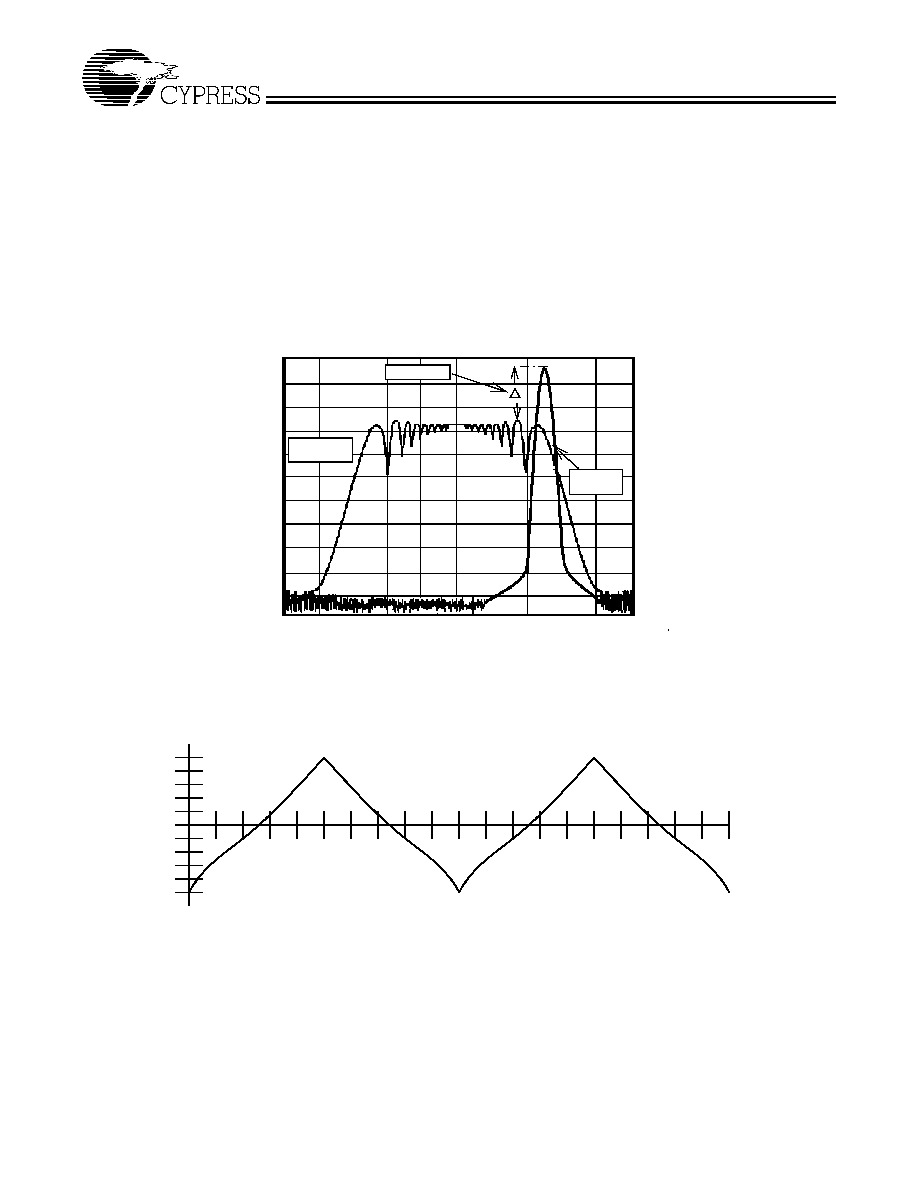
The device generates a clock that is frequency modulated in
order to increase the bandwidth that it occupies. By increasing
the bandwidth of the fundamental and its harmonics, the am-
plitudes of the radiated electromagnetic emissions are re-
duced. This effect is depicted in Figure 5.
As shown in Figure 5, a harmonic of a modulated clock has a
much lower amplitude than that of an unmodulated signal. The
reduction in amplitude is dependent on the harmonic number
and the frequency deviation or spread. The equation for the
reduction is
dB = 6.5 + 9*log
10
(P) + 9*log
10
(F)
Where P is the percentage of deviation and F is the frequency
in MHz where the reduction is measured.
The output clock is modulated with a waveform depicted in
Figure 6. This waveform, as discussed in "Spread Spectrum
Clock Generation for the Reduction of Radiated Emissions" by
Bush, Fessler, and Hardin produces the maximum reduction
in the amplitude of radiated electromagnetic emissions. The
deviation selected for this chip is ≠0.5% of the selected fre-
quency. Figure 6 details the Cypress spreading pattern.
Cypress does offer options with more spread and greater EMI
reduction. Contact your local Sales representative for details
on these devices.
Spread
Spectrum
Enabled
EMI Reduction
Spread
Spectrum
Non-
Figure 5. Typical Clock and SSFTG Comparison
MAX.
MIN.
10%
20%
30%
40%
50%
60%
70%
80%
90%
1
00%
10%
20%
30%
40%
50%
60%
70%
80%
90%
1
00%
F
R
EQUENCY
Figure 6. Typical Modulation Profile