 | –≠–ª–µ–∫—Ç—Ä–æ–Ω–Ω—ã–π –∫–æ–º–ø–æ–Ω–µ–Ω—Ç: W210 | –°–∫–∞—á–∞—Ç—å:  PDF PDF  ZIP ZIP |
Spread Spectrum FTG for VIA K7 Chipset
W210
Cypress Semiconductor Corporation
∑
3901 North First Street
∑
San Jose
∑
CA 95134
∑
408-943-2600
April 11, 2000, rev. *C
Features
∑ Maximized EMI Suppression using Cypress's Spread
Spectrum technology
∑ Single-chip system frequency synthesizer for VIA K7
chipset
∑ One pair of differential CPU outputs for K7 Processor
∑ One open-drain CPU output for VIA K7 chipset
∑ Six copies of PCI output
∑ One 48-MHz output for USB
∑ One 24-MHz or 48-MHz output for SIO
∑ Two buffered reference outputs
∑ Thirteen SDRAM outputs provide support for 3 DIMMs
∑ Supports frequencies up to 200 MHz
∑ I
2
CTM interface for programming
∑ Power management control inputs
∑ Available in 48-pin SSOP
Key Specifications
CPU to CPU Output Skew: ......................................... 175 ps
PCI to PCI Output Skew: ............................................ 500 ps
V
DDQ3
: .................................................................... 3.3V±5%
I
2
C is a trademark of Philips Corporation.
Table 1. Mode Input Table
Mode
Pin 2
0
CPU_STOP#
1
REF0
Table 2. Pin Selectable Frequency
Input Address
CPU
(MHz)
PCI0:5
(MHz)
Spread
Spectrum
FS3 FS2 FS1 FS0
1
1
1
1
133.3
33.3 ±0.5%
1
1
1
0
75
37.5 ±0.5%
1
1
0
1
100.2
33.3
±0.5%
1
1
0
0
66.8
33.4
±0.5%
1
0
1
1
79
39.5
OFF
1
0
1
0
110
36.7
OFF
1
0
0
1
115
38.3
OFF
1
0
0
0
120
30
OFF
0
1
1
1
133.3
33.3
OFF
0
1
1
0
83.3
27.7
OFF
0
1
0
1
100.2
33.3
OFF
0
1
0
0
66.8
33.4
OFF
0
0
1
1
124
31.0
OFF
0
0
1
0
129
32.3
OFF
0
0
0
1
138
34.5
OFF
0
0
0
0
143
35.8
OFF
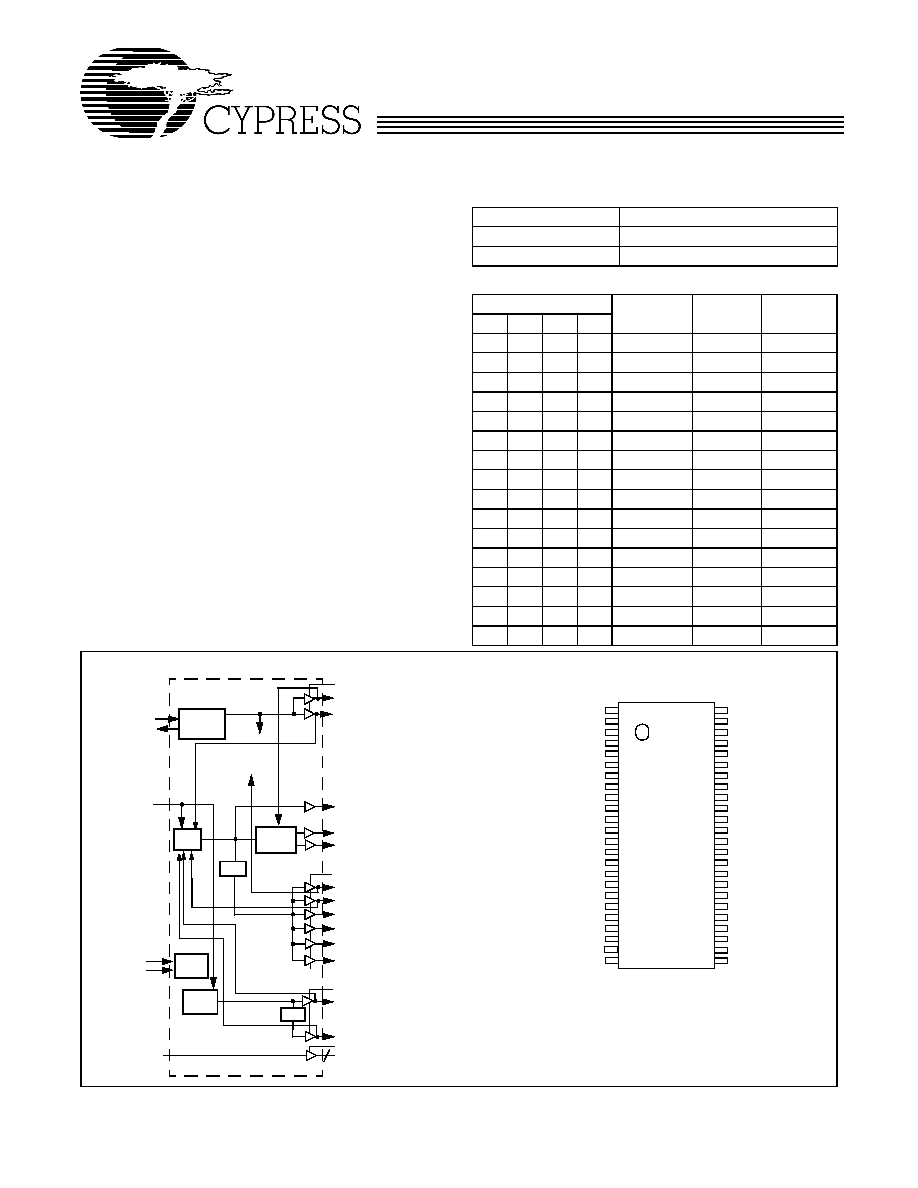
Block Diagram
Pin Configuration
Note:
1.
Internal pull-up resistors should not be relied upon for setting I/O
pins HIGH. Pin function with parentheses determined by MODE pin
resistor strapping. Unlike other I/O pins, input FS3 has an internal
pull-down resistor.
[1]
VDDQ3
REF0/(CPU_STOP#)
PCI0/MODE
XTAL
PLL Ref Freq
PLL 1
X2
X1
REF1/FS0
VDDQ3
Stop
Clock
Control
PCI2
PCI3
PCI4
48MHz/FS2
24_48MHz/FS3
PLL2
˜2,3,4
OSC
PWRDWN#
VDDQ3
PCI5
I
2
C
SDATA
Logic
SCLK
I/O Pin
Control
SDRAM0:12
SDRAMIN
13
VDDQ3
PCI1/FS1
CPUT0
˜2
CPUT_CS
CPUC0
VDDQ3
REF0/(CPU_STOP#)
GND
X1
X2
VDDQ3
PCI0/MODE
PCI1/FS1*
GND
PCI2
PCI3
PCI4
PCI5
VDDQ3
SDRAMIN
GND
SDRAM11
SDRAM10
VDDQ3
SDRAM9
SDRAM8
GND
SDATA
SCLK
W2
10
REF1/FS0*
GND
CPUT_CS
GND
CPUC0
CPUT0
VDDQ3
PWRDWN#*
SDRAM12
GND
SDRAM0
SDRAM1
VDDQ3
SDRAM2
SDRAM3
GND
SDRAM4
SDRAM5
VDDQ3
SDRAM6
SDRAM7
VDDQ3
48MHz/FS2*
24_48MHz/FS3^
48
47
46
45
44
43
42
41
40
39
38
37
36
35
34
33
32
31
30
29
28
27
26
25
1
2
3
4
5
6
7
8
9
10
11
12
13
14
15
16
17
18
19
20
21
22
23
24
I
2
C
{
W210
2
Pin Definitions
Pin Name
Pin No.
Pin Type
Pin Description
CPUT0,
CPUC0,
CPUT_CS
43, 44, 46
O
(open-
drain)
CPU Clock Output 0: CPUT0 and CPUC0 are the differential CPU clock outputs
for the K7 processor. CPUT_CS is the open-drain clock output for the chipset. It
has the same phase relationship as CPUT0.
PCI2:5
10, 11, 12, 13
O
PCI Clock Outputs 2 through 5: These four PCI clock outputs are controlled by
the PWRDWN# control pin. Frequency is set by FS0:3 inputs or through serial
input interface, see Tables 2 and 6 for details. Output voltage swing is controlled
by voltage applied to VDDQ3.
PCI1/FS1
8
I/O
Fixed PCI Clock Output/Frequency Select 1: As an output, frequency is set by
FS0:3 inputs or through serial input interface. This output is controlled by the
PWRDWN# input. This pin also serves as a power-on strap option to determine
device operating frequency as described in Table 2.
PCI0/MODE
7
I/O
Fixed PCI Clock Output/Mode: As an output, frequency is set by the FS0:3 inputs
or through serial input interface, see Tables 2 and 6. This output is controlled by
the PWRDWN# input. This pin also serves as a power-on strap option to determine
the function of pin 2, see Table 1 for details.
PWRDWN#
41
I
PWRDWN# Input: LVTTL-compatible input that places the device in power-down
mode when held LOW. In power-down mode,CPUC0 will be three-stated and all
the other output clocks will be driven LOW.
48MHz/FS2
26
I/O
48-MHz Output/Frequency Select 2: 48 MHz is provided in normal operation. In
standard PC systems, this output can be used as the reference for the Universal
Serial Bus host controller. This pin also serves as a power-on strap option to
determine device operating frequency as described in Table 2.
24_48MHz/
FS3
25
I/O
24_48-MHz Output/Frequency Select 3: In standard PC systems, this output can
be used as the clock input for a Super I/O chip. The output frequency is controlled
by Configuration Byte 3 bit[6]. The default output frequency is 24 MHz. This pin
also serves as a power-on strap option to determine device operating frequency
as described in Table 2.
REF1/FS0
48
I/O
Reference Clock Output 1/Frequency Select 2: 3.3V 14.318-MHz output clock.
This pin also serves as a power-on strap option to determine device operating
frequency as described in Table 2. Upon power-up, FS0 input will be latched, which
will set clock frequencies as described in Table 2.
REF0/
CPU_STOP#
2
I/O
Reference Clock Output 0 or CPU_STOP# Input Pin: Function is determined
by the MODE pin. When CPU_STOP# input is asserted LOW, it will drive CPUT0
and CPUT_CS to logic 0, and it will three-state CPUC0. When this pin is configured
as an output, this pin becomes a 3.3V 14.318-MHz output clock.
SDRAMIN
15
I
Buffered Input Pin: The signal provided to this input pin is buffered to 13 outputs
(SDRAM0:12).
SDRAM0:12
38, 37, 35,
34, 32, 31,
29, 28, 21,
20, 18, 17, 40
O
Buffered Outputs: These thirteen dedicated outputs provide copies of the signal
provided at the SDRAMIN input. The swing is set by VDDQ3, and they are deac-
tivated when PWRDWN# input is set LOW.
SCLK
24
I
Clock pin for I
2
C circuitry.
SDATA
23
I/O
Data pin for I
2
C circuitry.
X1
4
I
Crystal Connection or External Reference Frequency Input: This pin has dual
functions. It can be used as an external 14.318-MHz crystal connection or as an
external reference frequency input.
X2
5
I
Crystal Connection: An input connection for an external 14.318-MHz crystal. If
using an external reference, this pin must be left unconnected.
VDDQ3
1, 6, 14, 19,
27, 30, 36, 42
P
Power Connection: Power supply for core logic, PLL circuitry, SDRAM outputs,
PCI outputs, reference outputs, 48-MHz output, and 24_48-MHz output. Connect
to 3.3V supply.
GND
3, 9, 16, 22,
33, 39, 45, 47
G
Ground Connections: Connect all ground pins to the common system ground
plane.
W210
3
Overview
The W210 was developed as a single-chip device to meet the
clocking needs of VIA K7 core logic chip sets. In addition to the
typical outputs provided by a standard FTG, the W210 adds a
thirteenth output buffer, supporting SDRAM DIMM modules in
conjunction with the chipset.
Cypress's proprietary spread spectrum frequency synthesis
technique is a feature of the CPU and PCI outputs. When en-
abled, this feature reduces the peak EMI measurements of not
only the output signals and their harmonics, but also of any
other clock signals that are properly synchronized to them.
Functional Description
I/O Pin Operation
Pins 7, 8, 25, 26, and 48 are dual-purpose l/O pins. Upon
power-up these pins act as logic inputs, allowing the determi-
nation of assigned device functions. A short time after power-
up, the logic state of each pin is latched and the pins become
clock outputs. This feature reduces device pin count by com-
bining clock outputs with input select pins.
An external 10-k
"strapping" resistor is connected between
the l/O pin and ground or V
DD
. Connection to ground sets a
latch to "0," connection to V
DD
sets a latch to "1." Figure 1 and
Figure 2 show two suggested methods for strapping resistor
connections.
Upon W210 power-up, the first 2 ms of operation is used for
input logic selection. During this period, the five I/O pins (7, 8,
25, 26, 48) are three-stated, allowing the output strapping re-
sistor on the l/O pins to pull the pins and their associated ca-
pacitive clock load to either a logic HIGH or LOW state. At the
end of the 2-ms period, the established logic "0" or "1" condi-
tion of the l/O pin is latched. Next the output buffer is enabled
converting the l/O pins into operating clock outputs. The 2-ms
timer starts when V
DD
reaches 2.0V. The input bits can only
be reset by turning V
DD
off and then back on again.
It should be noted that the strapping resistors have no signifi-
cant effect on clock output signal integrity. The drive imped-
ance of clock outputs is <40
(nominal), which is minimally
affected by the 10-k
strap to ground or V
DD
. As with the se-
ries termination resistor, the output strapping resistor should
be placed as close to the l/O pin as possible in order to keep
the interconnecting trace short. The trace from the resistor to
ground or V
DD
should be kept less than two inches in length to
prevent system noise coupling during input logic sampling.
When the clock outputs are enabled following the 2-ms input
period, the specified output frequency is delivered on the pin,
assuming that V
DD
has stabilized. If V
DD
has not yet reached
full value, output frequency initially may be below target but will
increase to target once V
DD
voltage has stabilized. In either
case, a short output clock cycle may be produced from the
CPU clock outputs when the outputs are enabled.
Power-on
Reset
Timer
Output Three-state
Data
Latch
Hold
Q
D
W210
V
DD
Clock Load
R
10 k
Output
Buffer
(Load Option 1)
10 k
(Load Option 0)
Output
Low
Output Strapping Resistor
Series Termination Resistor
Figure 1. Input Logic Selection Through Resistor Load Option
Power-on
Reset
Timer
Output Three-state
Data
Latch
Hold
Q
D
W210
V
DD
Clock Load
R
10 k
Output
Buffer
Output
Low
Output Strapping Resistor
Series Termination Resistor
Jumper Options
Figure 2. Input Logic Selection Through Jumper Option
Resistor Value R
W210
4
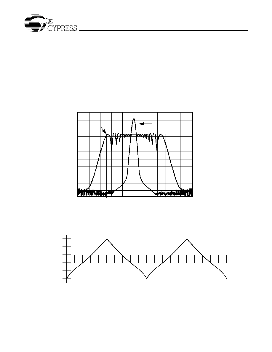
Spread Spectrum Frequency Timing Generator
The device generates a clock that is frequency modulated in
order to increase the bandwidth that it occupies. By increasing
the bandwidth of the fundamental and its harmonics, the am-
plitudes of the radiated electromagnetic emissions are re-
duced. This effect is depicted in Figure 3.
As shown in Figure 3, a harmonic of a modulated clock has a
much lower amplitude than that of an unmodulated signal. The
reduction in amplitude is dependent on the harmonic number
and the frequency deviation or spread. The equation for the
reduction is:
dB = 6.5 + 9*log
10
(P) + 9*log
10
(F)
Where P is the percentage of deviation and F is the frequency
in MHz where the reduction is measured.
The output clock is modulated with a waveform depicted in
Figure 4. This waveform, as discussed in "Spread Spectrum
Clock Generation for the Reduction of Radiated Emissions" by
Bush, Fessler, and Hardin produces the maximum reduction
in the amplitude of radiated electromagnetic emissions. The
deviation selected for this chip is specified in Table 6. Figure 4
details the Cypress spreading pattern. Cypress does offer op-
tions with more spread and greater EMI reduction. Contact
your local Sales representative for details on these devices.
Spread Spectrum clocking is activated or deactivated by se-
lecting the appropriate values for bits 1≠0 in data byte 0 of the
I
2
C data stream. Refer to Table 6 for more details.
Figure 3. Clock Harmonic with and without SSCG Modulation Frequency Domain Representation
SSFT G
Typical C lo ck
Freq uency S pan (M H z)
-S S%
+ SS %
A
m
pl
i
t
ude
(
d
B
)
5 d B /d iv
Figure 4. Typical Modulation Profile
MAX (0%)
MIN (≠0.5%)
10%
20%
30%
40%
50%
60%
70%
80%
90%
100%
10%
20%
30%
40%
50%
60%
70%
80%
90%
100%
FREQUENCY
W210
5
Serial Data Interface
The W210 features a two-pin, serial data interface that can be
used to configure internal register settings that control partic-
ular device functions. Upon power-up, the W210 initializes with
default register settings, therefore the use of this serial data
interface is optional. The serial interface is write-only (to the
clock chip) and is the dedicated function of device pins SDATA
and SCLOCK. In motherboard applications, SDATA and
SCLOCK are typically driven by two logic outputs of the
chipset. Clock device register changes are normally made
upon system initialization, if any are required. The interface
can also be used during system operation for power manage-
ment functions. Table 3 summarizes the control functions of
the serial data interface.
Operation
Data is written to the W210 in eleven bytes of eight bits each.
Bytes are written in the order shown in Table 4.
Table 3. Serial Data Interface Control Functions Summary
Control Function
Description
Common Application
Clock Output Disable
Any individual clock output(s) can be disabled. Dis-
abled outputs are actively held LOW.
Unused outputs are disabled to reduce EMI
and system power. Examples are clock out-
puts to unused PCI slots.
CPU Clock Frequency
Selection
Provides CPU/PCI frequency selections through
software. Frequency is changed in a smooth and
controlled fashion.
For alternate microprocessors and power
management options. Smooth frequency tran-
sition allows CPU frequency change under
normal system operation.
Spread Spectrum
Enabling
Enables or disables spread spectrum clocking.
For EMI reduction.
Output Three-state
Puts clock output into a high impedance state.
Production PCB testing.
(Reserved)
Reserved function for future device revision or pro-
duction device testing.
No user application. Register bit must be writ-
ten as 0.
Table 4. Byte Writing Sequence
Byte Sequence
Byte Name
Bit Sequence
Byte Description
1
Slave Address
11010010
Commands the W210 to accept the bits in Data Bytes 0≠6 for internal
register configuration. Since other devices may exist on the same com-
mon serial data bus, it is necessary to have a specific slave address for
each potential receiver. The slave receiver address for the W210 is
11010010. Register setting will not be made if the Slave Address is not
correct (or is for an alternate slave receiver).
2
Command
Code
Don't Care
Unused by the W210, therefore bit values are ignored ("Don't Care").
This byte must be included in the data write sequence to maintain proper
byte allocation. The Command Code Byte is part of the standard serial
communication protocol and may be used when writing to another ad-
dressed slave receiver on the serial data bus.
3
Byte Count
Don't Care
Unused by the W210, therefore bit values are ignored ("Don't Care").
This byte must be included in the data write sequence to maintain proper
byte allocation. The Byte Count Byte is part of the standard serial com-
munication protocol and may be used when writing to another addressed
slave receiver on the serial data bus.
4
Data Byte 0
Refer to Table 5
The data bits in Data Bytes 0≠7 set internal W210 registers that control
device operation. The data bits are only accepted when the Address
Byte bit sequence is 11010010, as noted above. For description of bit
control functions, refer to Table 5, Data Byte Serial Configuration Map.
5
Data Byte 1
6
Data Byte 2
7
Data Byte 3
8
Data Byte 4
9
Data Byte 5
10
Data Byte 6
11
Data Byte 7