 | –≠–ª–µ–∫—Ç—Ä–æ–Ω–Ω—ã–π –∫–æ–º–ø–æ–Ω–µ–Ω—Ç: W215B | –°–∫–∞—á–∞—Ç—å:  PDF PDF  ZIP ZIP |
PRELIMINARY
Notebook PC System Frequency Generator for K6 Processors
W215B
Cypress Semiconductor Corporation
∑
3901 North First Street
∑
San Jose
∑
CA 95134
∑
408-943-2600
December 27, 1999, rev. **
Features
∑ Generates system clocks for CPU, IOAPIC, SDRAM,
PCI, USB plus 14.318 MHz (REF0:1)
∑ MODE input pin selects optional power management
input control pins (reconfigures pins 26 and 27)
∑ Two fixed outputs separately selectable as 24-MHz or
48-MHz (default = 48-MHz)
∑ V
DDQ3
= 3.3V±5%, V
DDQ2
= 3.3V±5%
∑ Uses external 14.318-MHz crystal
∑ Available in 48-pin TSSOP (6.1-mm)
∑ 10
CPU output impedance
Table 1. Pin Selectable Frequency
95/100_SEL
CPU, SDRAM
Clocks (MHz)
PCI Clocks
0
95.0
CPU/3
1
100.0
CPU/3
Pin Configuration
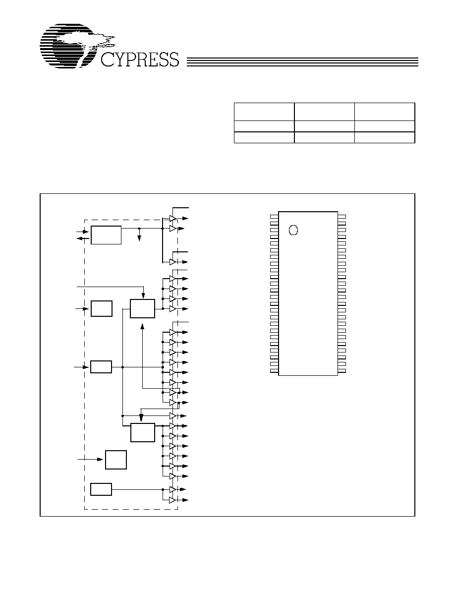
Block Diagram
VDDQ3
REF0
VDDQ2
IOAPIC
CPU0
CPU1
CPU2
CPU3
SDRAM0
SDRAM1
SDRAM2
SDRAM3
SDRAM4
SDRAM5
SDRAM6/CPUSTOP#
SDRAM7/PCISTOP#
PCI_F
PCI0
XTAL
PLL Ref Freq
PLL 1
95/100_SEL
MODE
X2
X1
REF1
VDDQ3
Stop
Output
Control
Stop
Output
Control
PCI1
PWR_DWN#
Power
Down
Control
PCI2
PCI3
PCI4
PCI5
48/24MHZ
48/24MHZ
PLL2
OSC
I/O
Control
VDDQ2
REF1
REF0
GND
X1
X2
MODE
VDDQ3
PCI_F
PCI0
GND
PCI1
PCI2
PCI3
PCI4
VDDQ3
PCI5
GND
95/100_SEL
Reserved
Reserved
VDDQ3
48/24MHZ
48/24MHZ
GND
W2
15B
VDDQ3
CPU_2.5#
VDDQ2
IOAPIC
PWR_DWN#
GND
CPU0
CPU1
VDDQ2
CPU2
CPU3
GND
SDRAM0
SDRAM1
VDDQ3
SDRAM2
SDRAM3
GND
SDRAM4
SDRAM5
VDDQ3
SDRAM6/CPU_STOP#
SDRAM7/PCI_STOP#
VDDQ3
48
47
46
45
44
43
42
41
40
39
38
37
36
35
34
33
32
31
30
29
28
27
26
25
1
2
3
4
5
6
7
8
9
10
11
12
13
14
15
16
17
18
19
20
21
22
23
24
CPU_2.5#
W215B
PRELIMINARY
2
Pin Definitions
Pin Name
Pin
No.
Pin
Type
Pin Description
CPU0:3
42, 41, 39,
38
O
CPU Outputs 0 through 3: These four CPU outputs are controlled by the
CPU_STOP# control pin. Output voltage swing is controlled by voltage applied to
VDDQ2.
PCI0:5
9, 11, 12,
13, 14, 16
O
PCI Bus Outputs 0 through 5: These six PCI outputs are controlled by the
PCI_STOP# control pin. Output voltage swing is controlled by voltage applied to
VDDQ3.
PCI_F
8
O
Free Running PCI Output: Unlike PCI0:5 outputs, this output is not controlled by the
PCI_STOP# control pin. Output voltage swing is controlled by voltage applied to
VDDQ3.
SDRAM0:5
36, 35, 33,
32, 30, 29
O
SDRAM Clock Outputs 0 through 5: These six SDRAM clock outputs run synchro-
nous to the CPU clock outputs. Output voltage swing is controlled by voltage applied
to VDDQ3.
SDRAM6/
CPU_STOP#
27
I/O
SDRAM Clock Output 6 or CPU Clock Output Stop Control: This pin has dual
functions, selectable by the MODE input pin. When MODE = 0, this pin becomes the
CPU_STOP# input. When MODE = 1, this pin becomes SDRAM clock output 6.
Regarding use as a CPU_STOP# input: When brought LOW, clock outputs CPU0:3
are stopped LOW after completing a full clock cycle (2≠3 CPU clock latency). When
brought HIGH, clock outputs CPU0:3 are started beginning with a full clock cycle (2≠3
CPU clock latency).
Regarding use as a SDRAM clock: Output voltage swing is controlled by voltage ap-
plied to VDDQ3.
SDRAM7/
PCI_STOP#
26
I/O
SDRAM Clock Output 7 or PCI Clock Output Stop Control: This pin has dual
functions, selectable by the MODE input pin. When MODE = 0, this pin becomes the
PCI_STOP# input. When MODE = 1, this pin becomes SDRAM clock output 7.
PCI_STOP# input: When brought LOW, clock outputs PCI0:5 are stopped LOW after
completing a full clock cycle. When brought HIGH, clock outputs PCI0:5 are started
beginning with a full clock cycle. Clock latency provides one PCI_F rising edge of PCI
clock following PCI_STOP# state change.
Regarding use as a SDRAM clock: Output voltage swing is controlled by voltage ap-
plied to VDDQ3.
IOAPIC
45
O
I/O APIC Clock Output: Provides 14.318-MHz fixed frequency. The output voltage
swing is controlled by VDDQ2.
48/24MHz
22, 23
O
48-MHz / 24-MHz Output: Fixed clock outputs that default to 48 MHz following device
power-up. Either or both can be changed to 24 MHz through use of the serial data
interface (Byte 0, bits 2 and 3). Output voltage swing is controlled by voltage applied
to VDDQ3
REF0:1
2, 1
O
Fixed 14.318-MHz Outputs 0 through 1: Used for various system applications. Out-
put voltage swing is controlled by voltage applied to VDDQ3. REF0 is stronger than
REF1 and should be used for driving ISA slots.
CPU_2.5#
47
I
Set to logic 1 for 3.3V CPU I/O.
95/100_SEL
18
I
95- or 100-MHz Input Selection: Selects power-up default CPU clock frequency as
shown in Table 1 on page 1 (also determines SDRAM and PCI clock frequency selec-
tions).
X1
4
I
Crystal Connection or External Reference Frequency Input: This pin has dual
functions. It can be used as an external 14.318-MHz crystal connection or as an
external reference frequency input.
X2
5
I
Crystal Connection: An input connection for an external 14.318-MHz crystal. If using
an external reference, this pin must be left unconnected.

W215B
PRELIMINARY
3
PWR_DWN#
44
I
Power-Down Control: When this input is LOW, device goes into a low-power standby
condition. All outputs are actively held LOW while in power-down. CPU, SDRAM, and
PCI clock outputs are stopped LOW after completing a full clock cycle (2≠4 CPU clock
cycle latency). When brought HIGH, CPU, SDRAM, and PCI outputs start with a full
clock cycle at full operating frequency (3 ms maximum latency).
MODE
6
I
Mode Control: This input selects the function of device pin 26 (SDRAM7/PCI_STOP#)
and pin 27 (SDRAM6/CPU_STOP#). Refer to description for those pins.
VDDQ3
7, 15, 21, 25
28, 34, 48
P
Power Connection: Power supply for PCI0:5, REF0:1, and 48-/24-MHz output buffers.
Connected to 3.3V supply.
VDDQ2
46, 40
P
Power Connection: Power supply for IOAPIC0, CPU0:3 output buffer. Connected to
3.3V supply.
GND
3, 10, 17,
24, 31, 37,
43
G
Ground Connection: Connect all ground pins to the common system ground plane.
Reserved
19, 20
I
Reserved Pins: Connect to Logic 1.
Pin Definitions
Pin Name
Pin
No.
Pin
Type
Pin Description
W215B
PRELIMINARY
4
Absolute Maximum Ratings
Stresses greater than those listed in this table may cause per-
manent damage to the device. These represent a stress rating
only. Operation of the device at these or any other conditions
above those specified in the operating sections of this specifi-
cation is not implied. Maximum conditions for extended peri-
ods may affect reliability.
Parameter
Description
Rating
Unit
V
DD
, V
IN
Voltage on any pin with respect to GND
≠0.5 to +7.0
V
T
STG
Storage Temperature
≠65 to +150
∞C
T
B
Ambient Temperature under Bias
≠55 to +125
∞C
T
A
Operating Temperature
0 to +70
∞C
ESD
PROT
Input ESD Protection
2 (min.)
kV
DC Electrical Characteristics
T
A
= 0∞C to +70∞C, V
DDQ3
= 3.3V±5% (3.135≠3.465V), f
XTL
= 14.31818 MHz, V
DDQ2
= 3.3V±5%
Parameter
Description
Test Condition
Min.
Typ.
Max.
Unit
Supply Current
I
DDQ3
Supply Current (3.3V)
CPU0:3 = 100 MHz
Outputs Loaded
[1]
150
mA
I
DDQ2
Supply Current (3.3V)
CPU0:3 = 100 MHz
Outputs Loaded
[1]
80
mA
Logic Inputs
V
IL
Input Low Voltage
0.8
V
V
IH
Input High Voltage
2.0
V
I
IL
Input Low Current
[2]
10
µA
I
IH
Input High Current
[2]
10
µA
Clock Outputs
V
OL
Output Low Voltage
I
OL
= 2 mA
50
mV
V
OH
Output High Voltage
I
OH
= ≠1 mA
3.1
V
I
OL
Output Low Current
CPU0:3
V
OL
= 1.5V
140
mA
SDRAM0:7
V
OL
= 1.5V
110
mA
PCI_F, PCI0:5
V
OL
= 1.5V
110
mA
IOAPIC
V
OL
= 1.5V
95
mA
REF0
V
OL
= 1.5V
75
mA
REF1
V
OL
= 1.5V
70
mA
48/24MHZ
V
OL
= 1.5V
70
mA
I
OH
Output High Current
CPU0:3
V
OL
= 1.5V
120
mA
SDRAM0:7
V
OL
= 1.5V
95
mA
PCI_F, PCI0:5
V
OL
= 1.5V
95
mA
IOAPIC
V
OL
= 1.5V
95
mA
REF0
V
OL
= 1.5V
80
mA
REF1
V
OL
= 1.5V
62
mA
48/24MHZ
V
OL
= 1.5V
60
mA
Notes:
1.
All clock outputs loaded with maximum lump capacitance test load specified in AC Electrical Characteristics section.
2.
W215B logic inputs have internal pull-up devices (not CMOS level).

W215B
PRELIMINARY
5
AC Electrical Characteristics (Lump Load Model)
T
A
= 0∞C to +70∞C, V
DDQ3
= 3.3V±5% (3.135≠3.465V) f
XTL
= 14.31818 MHz, V
DDQ2
= 3.3V±5%
AC clock parameters are tested and guaranteed over stated operating conditions using the stated lump capacitive load at the
clock output.
Crystal Oscillator
V
TH
X1 Input Threshold Voltage
[3]
V
DDQ3
= 3.3V
1.65
V
C
LOAD
Load Capacitance, Imposed on External
Crystal
[4]
14
pF
C
IN,X1
X1 Input Capacitance
[5]
Pin X2 unconnected
28
pF
Pin Capacitance/Inductance
C
IN
Input Pin Capacitance
Except X1 and X2
5
pF
C
OUT
Output Pin Capacitance
6
pF
L
IN
Input Pin Inductance
7
nH
Notes:
3.
X1 input threshold voltage (typical) is V
DDQ3
/2.
4.
The W215B contains an internal crystal load capacitor between pin X1 and ground and another between pin X2 and ground. Total load placed on crystal is
14 pF; this includes typical stray capacitance of short PCB traces to crystal.
5.
X1 input capacitance is applicable when driving X1 with an external clock source (X2 is left unconnected).
DC Electrical Characteristics
(continued)
T
A
= 0∞C to +70∞C, V
DDQ3
= 3.3V±5% (3.135≠3.465V), f
XTL
= 14.31818 MHz, V
DDQ2
= 3.3V±5%
Parameter
Description
Test Condition
Min.
Typ.
Max.
Unit
F T G
Test Point
* 2 0 p F f o r C P U , R E F 1 , I O A P I C ,
2 4 M H z & 4 8 M H z
* 3 0 p F f o r S D R A M & P C I
CPU Clock Outputs, CPU0:3 (Lump Capacitance Test Load = 20 pF)
Parameter
Description
Test Condition/Comments
CPU = 100 MHz
Unit
Min.
Typ.
Max.
t
P
Period
Measured on rising edge at 1.5V
10
ns
f
Frequency, Actual
Determined by PLL divider ratio
100
MHz
t
H
High Time
Duration of clock cycle above 2.4V
5
ns
t
L
Low Time
Duration of clock cycle below 0.4V
5
ns
t
R
Output Rise Edge Rate
Measured from 0.4V to 2.4V
1
4
V/ns
t
F
Output Fall Edge Rate
Measured from 2.4V to 0.4V
1
4
V/ns
t
D
Duty Cycle
Measured on rising and falling edge at 1.5V
45
50
55
%
t
JC
Jitter, Cycle-to-Cycle
Measured on rising edge at 1.5V. Maximum differ-
ence of cycle time between two adjacent cycles.
500
ps
t
SK
Output Skew
Measured on rising edge at 1.5V
250
ps
f
ST
Frequency Stabilization from
Power-up (cold start)
Assumes full supply voltage reached within 1 ms
from power-up. Short cycles exist prior to frequency
stabilization.
3
ms
Z
o
AC Output Impedance
Average value during switching transition. Used for
determining series termination value.
10