 | –≠–ª–µ–∫—Ç—Ä–æ–Ω–Ω—ã–π –∫–æ–º–ø–æ–Ω–µ–Ω—Ç: W228BH | –°–∫–∞—á–∞—Ç—å:  PDF PDF  ZIP ZIP |
FTG for Integrated Core Logic with 133-MHz FSB
W228B
Cypress Semiconductor Corporation
∑
3901 North First Street
∑
San Jose
∑
CA 95134
∑
408-943-2600
Document #: 38-07180 Rev. *A
Revised December 22, 2002
Features
∑ Maximized EMI suppression using Cypress's Spread
Spectrum technology
∑ Two copies of CPU clock at 66/100/133 MHz
∑ Thirteen copies of 100-MHz SDRAM clocks
∑ Two copies of PCI clock
∑ One copy of APIC clock at 33 MHz, synchronous to CPU
clock
∑ Two copies of 48-MHz clock (non-spread spectrum) op-
timized for USB reference input and video dot clock
∑ Three copies of 3V 66-MHz fixed clock
∑ One copy of 14.31818-MHz reference clock
∑ Power down control
∑ SMBus interface for turning off unused clocks
Key Specifications
CPU, SDRAM Outputs Cycle-to-Cycle Jitter:.............. 250 ps
APIC, 48-MHz, 3V66, PCI Outputs
Cycle-to-Cycle Jitter:................................................... 500 ps
APIC, SDRAM Output Skew: ...................................... 250 ps
CPU, 3V66 Output Skew: ............................................ 175 ps
PCI Output Skew: ........................................................ 500 ps
CPU to SDRAM Skew (@ 133 MHz):.........................±0.5 ns
CPU to SDRAM Skew (@ 100 MHz):................. 4.5 to 5.5 ns
CPU to 3V66 Skew (@ 66 MHz): ....................... 7.0 to 8.0 ns
3V66 to PCI Skew (3V66 lead):..........................1.5 to 3.5 ns
PCI to APIC Skew: .....................................................±0.5 ns
Intel is a registered trademark of Intel Corporation.
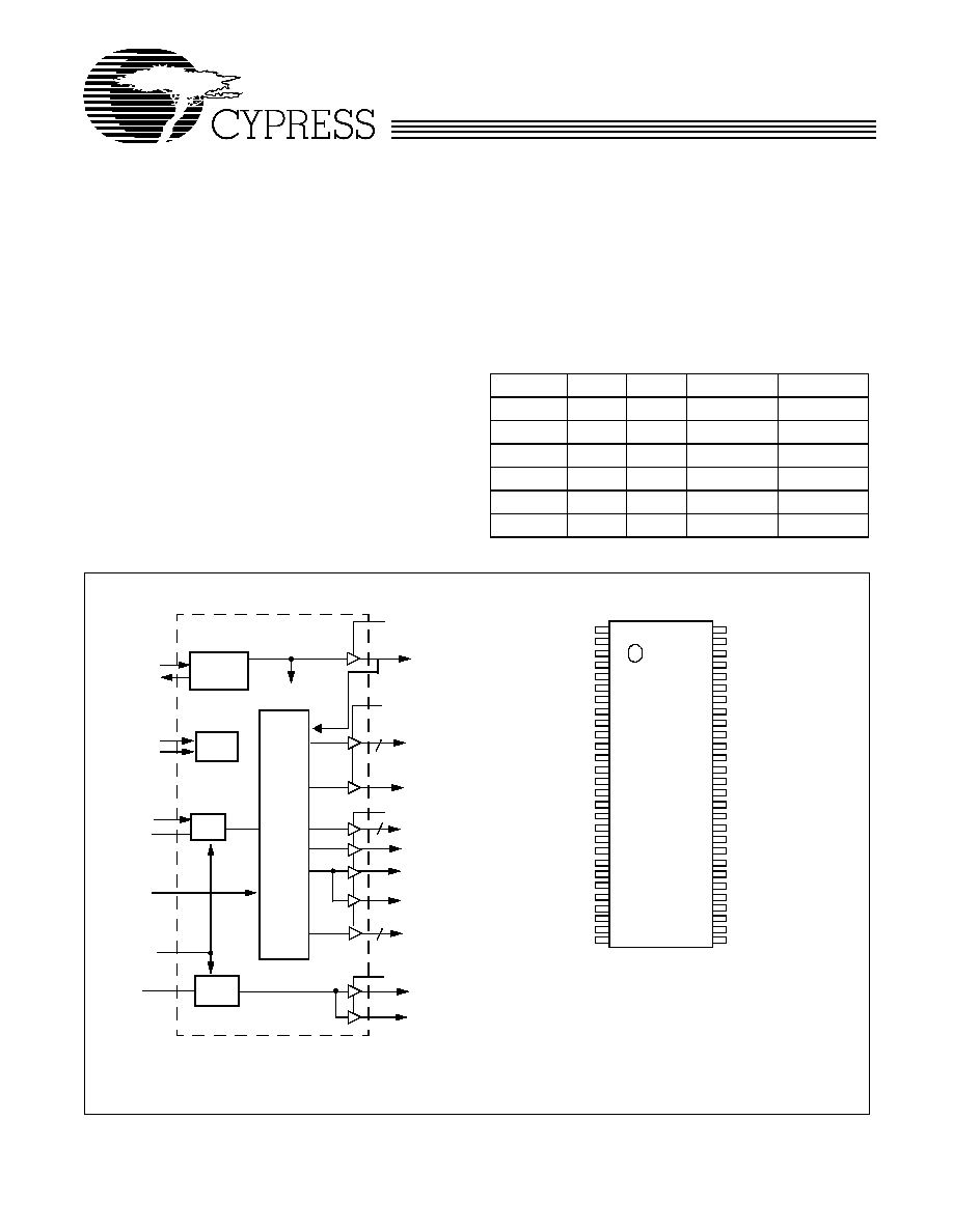
Table 1. Pin Selectable Functions
Tristate#
FSEL0
FSEL1
CPU
SDRAM
0
0
x
Three-state
Three-state
0
1
x
Test
Test
1
0
0
66 MHz
100 MHz
1
1
0
100 MHz
100 MHz
1
0
1
133 MHz
133 MHz
1
1
1
133 MHz
100 MHz
Block Diagram
Pin Configuration
Note:
1.
Internal pull-down resistors present on input marked with *.
Design should not solely rely on internal pull-down resister to
set I/O pin LOW.
[1]
VDDQ3
VDDQ2
PCI0_ICH
XTAL
PLL REF FREQ
PLL 1
X2
X1
REF0/FSEL1
PCI1
USB
DOT
PLL2
OSC
VDDQ3
SMBus
SDATA
Logic
SCLK
3V66_0:1
CPU0:1
FSEL1:0
APIC
Divider,
Delay,
and
Phase
Control
Logic
2
VDDQ3
2
SDRAM0:12
13
PWRDWN#
VDDA
VDDA
3V66_AGP
Tristate#
APIC
VDDQ2
GND
REF0/FSEL1*
VDDQ3
X1
X2
GND
VDDQ3
3V66_0
3V66_1
3V66_AGP
GND
VDDQ3
PCI0_ICH
PCI1
GND
FSEL0
GNDA
VDDA
PWRDWN#
SCLK
SDATA
GND
W228
B
VDDQ2
GND
CPU0
CPU1
GND
SDRAM0
SDRAM1
VDDQ3
GND
SDRAM2
SDRAM3
SDRAM4
VDDQ3
GND
SDRAM5
SDRAM6
VDDQ3
GND
SDRAM7
SDRAM8
SDRAM9
VDDQ3
GND
SDRAM10
56
55
54
53
52
51
50
49
48
47
46
45
44
43
42
41
40
39
38
37
36
35
34
33
1
2
3
4
5
6
7
8
9
10
11
12
13
14
15
16
17
18
19
20
21
22
23
24
25
26
27
28
32
31
30
29
VDDQ3
USB
DOT
Tristate#
SDRAM11
VDDQ3
GND
SDRAM12
W228B
Document #: 38-07180 Rev. *A
Page 2 of 16
Pin Definitions
Pin Name
Pin No.
Pin
Type
Pin Description
REF0/FSEL1
4
I/O
Reference Clock: 3.3V 14.318-MHz clock output. This pin also serves as a strap
option for CPU frequency selection. See Table 1 for detailed descriptions.
X1
6
I
Crystal Input: This pin has dual functions. It can be used as an external
14.318-MHz crystal connection or as an external reference frequency input.
X2
7
O
Crystal Output: A connection for an external 14.318-MHz crystal. If using an ex-
ternal reference, this pin must be left unconnected.
PCI0_ICH,
PCI1
15, 16
O
PCI Clock 0 through 1: 3.3V 33-MHz PCI clock outputs. PCI1 can be individually
turned off via SMBus interface.
3V66_0:2,
3V66_AGP
10, 11, 12
O
66-MHz Clock Output: 3.3V fixed 66-MHz clock.
USB
26
O
USB Clock Output: 3.3V fixed 48-MHz, non-spread spectrum USB clock output.
DOT
27
O
Dot Clock Output: 3.3V 48-MHz, non-spread spectrum signal.
Tristate#,
FSEL0
28, 18
I
Clock Function Selection pins: LVTTL-compatible input to select device func-
tions. See Table 1 for detailed descriptions.
PWRDWN#
21
I
Power-Down Control: LVTTL-compatible asynchronous input that places the de-
vice in power-down mode when held LOW.
CPU0:1
54, 53
O
CPU Clock Outputs: Clock outputs for the host bus interface and integrated test
port. Output frequencies run at 66 MHz, 100 MHz, or 133 MHz depending on the
configuration of SEL0:1 and SEL133. Voltage swing set by VDDQ2.
SDRAM0:12
51, 50, 47, 46,
45, 42, 41, 38,
37, 36, 33, 32,
29
O
SDRAM Clock Outputs: 3.3V outputs running at 100 MHz. SDRAM0:12 can be
individually turned off via SMBus interface.
APIC
1
O
Synchronous APIC Clock Outputs: Clock outputs running synchronous with the
PCI clock outputs (33 MHz). Voltage swing set by VDDQ2.
SDATA
23
I/O
Data pin for SMBus circuitry.
SCLK
22
I
Clock pin for SMBus circuitry.
VDDQ3
5, 9, 14, 25, 31,
35, 40, 44, 49
P
3.3V Power Connection: Power supply for SDRAM output buffers, PCI output
buffers, 3V66 output buffers, reference output buffers, and 48-MHz output buffers.
Connect to 3.3V.
VDDA
20
P
3.3V Power Connection: Power supply for core logic, PLL circuitry. Connect to
3.3V.
VDDQ2
2, 56
P
2.5V Power Connection: Power supply for IOAPIC and CPU output buffers. Con-
nect to 2.5V or 3.3V.
GND
3, 8, 13, 17, 24,
30, 34, 39, 43,
48, 52, 55
G
Ground Connections: Connect all ground pins to the common system ground
plane.
GNDA
19
G
Ground Connections: Connect all ground pins to the common system ground
plane.
W228B
Document #: 38-07180 Rev. *A
Page 3 of 16
Overview
The W228B is a highly integrated frequency timing generator,
supplying all the required clock sources for an Intel
Æ
architec-
ture platform using graphics integrated core logic.
Functional Description
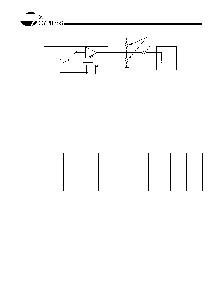
I/O Pin Operation
REF0/FSEL1 is a dual-purpose l/O pin. Upon power-up the pin
acts as a logic input for FSEL1 selection (see Table 1 and
Table 2). If the pin is strapped to a HIGH state externally, CPU
will be strapped LOW. CPU clock outputs will be determined
by the status of SEL0:1 input pins. An external 10-k
strapping
resistor should be used. Figure 1 shows a suggested method
for strapping resistor connections.
After 2 ms, the pin becomes an output. Assuming the power
supply has stabilized by then, the specified output frequency
is delivered on the pins. If the power supply has not yet
reached full value, output frequency initially may be below tar-
get but will increase to target once supply voltage has stabi-
lized. In either case, a short output clock cycle may be pro-
duced from the CPU clock outputs when the outputs are
enabled.
Pin Selectable Functions
Table 2 outlines the device functions selectable through
Tristate# and FSEL0:1. Specific outputs available at each pin
are detailed in Table 2 below.
Notes:
2.
Provided for board-level "bed of nails" testing.
3.
"Normal" mode of operation.
4.
TCLK is a test clock overdriven on the XTAL_IN input during test mode.
5.
Required for DC output impedance verification.
6.
Range of reference frequency allowed is min. = 14.316 MHz, nominal = 14.31818 MHz, max. = 14.32 MHz.
7.
Frequency accuracy of 48 MHz must be +167 PPM to match USB default.
Power-on
Reset
Timer
Output Three-state
Data
Latch
Hold
Q
D
W228B
V
DD
Clock Load
10 k
Output
Buffer
(Load Option 1)
10k
(Load Option 0)
Output
Low
Output Strapping Resistor
Series Termination Resistor
Figure 1. Input Logic Selection Through Resistor Load Option
Table 2. CK Whitney Truth Table
Tristate#
FSEL0
FSEL1
CPU
SDRAM
3V66
PCI
48MHz
REF
APIC
Notes
0
0
X
Hi-Z
Hi-Z
Hi-Z
Hi-Z
Hi-Z
Hi-Z
Hi-Z
2
0
1
X
TCLK/4
TCLK/4
TCLK/6
TCLK/12
TCLK/2
TCLK
TCLK/12
4, 5
1
0
0
66 MHz
100 MHz
66 MHz
33 MHz
48 MHz
14.318 MHz
33 MHz
3, 6, 7
1
1
0
100 MHz
100 MHz
66 MHz
33 MHz
48 MHz
14.318 MHz
33 MHz
3, 6, 7
1
0
1
133 MHz
133 MHz
66 MHz
33 MHz
48 MHz
14.318 MHz
33 MHz
3, 6, 7
1
1
1
133 MHz
100 MHz
66 MHz
33 MHz
48 MHz
14.318 MHz
33 MHz
3, 6, 7
W228B
Document #: 38-07180 Rev. *A
Page 4 of 16
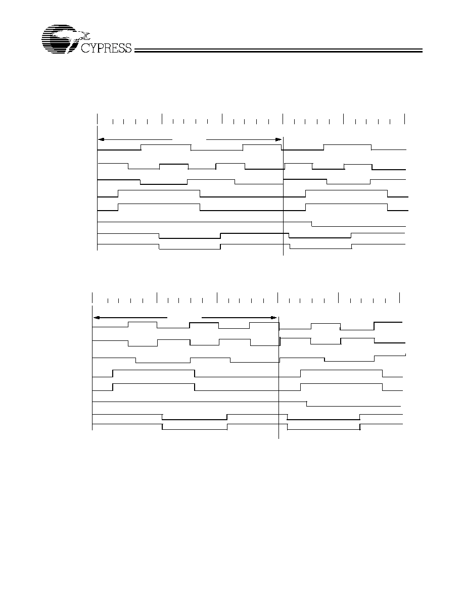
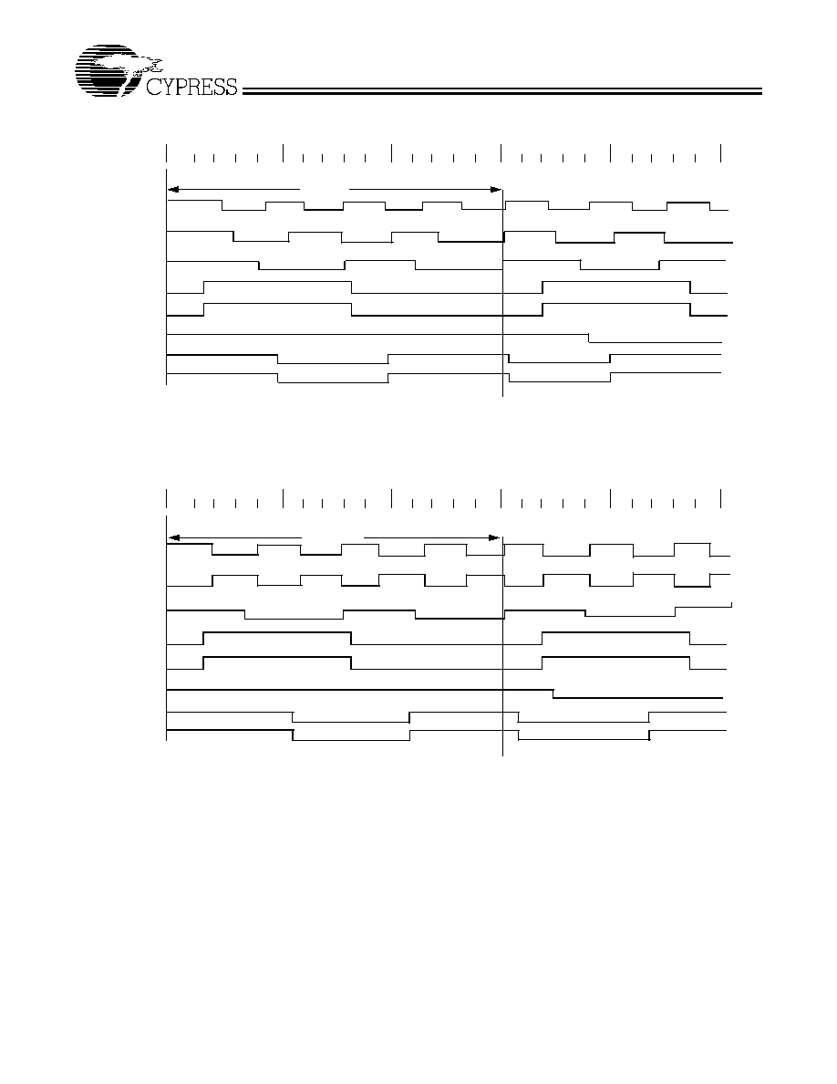
Offsets Among Clock Signal Groups
Figure 2 and Figure 3 represent the phase relationship among
the different groups of clock outputs from W228B when it is
providing a 66-MHz CPU clock and a 100-MHz CPU clock,
respectively. It should be noted that when the CPU clock is
operating at 100 MHz, CPU clock output is 180 degrees out of
phase with SDRAM clock outputs.
0 ns
Figure 2. Group Offset Waveforms (66-MHz CPU/100-MHz SDRAM Clock)
40 ns
30 ns
20 ns
10 ns
CPU 66-MHz
SDRAM 100-MHz
3V66 66-MHz
PCI 33-MHz
REF 14.318-MHz
USB 48-MHz
DOT 48-MHz
Cycle Repeat
APIC33-MHz
0 ns
Figure 3. Group Offset Waveforms (100-MHz CPU/100-MHz SDRAM Clock)
40 ns
30 ns
20 ns
10 ns
CPU 100-MHz
SDRAM 100-MHz
3V66 66-MHz
PCI 33-MHz
REF 14.318-MHz
USB 48-MHz
DOT 48-MHz
APIC 33-MHz
Cycle Repeat
W228B
Document #: 38-07180 Rev. *A
Page 5 of 16
0 ns
Figure 4. Group Offset Waveforms (133-MHz CPU/100-MHz SDRAM Clock)
40 ns
30 ns
20 ns
10 ns
CPU 133-MHz
SDRAM 100-MHz
3V66 66-MHz
PCI 33-MHz
REF 14.318-MHz
USB 48-MHz
DOT 48-MHz
Cycle Repeats
APIC 33-MHz
0 ns
Figure 5. Group Offset Waveforms (133-MHz CPU/133-MHz SDRAM Clock)
40 ns
30 ns
20 ns
10 ns
CPU 100-MHz
SDRAM 100-MHz
3V66 66-MHz
PCI 33-MHz
REF 14.318-MHz
USB 48-MHz
DOT 48-MHz
APIC 33-MHz
Cycle Repeat