 | –≠–ª–µ–∫—Ç—Ä–æ–Ω–Ω—ã–π –∫–æ–º–ø–æ–Ω–µ–Ω—Ç: W245-30 | –°–∫–∞—á–∞—Ç—å:  PDF PDF  ZIP ZIP |
Frequency Multiplying, Peak Reducing EMI Solution
W245-30
Cypress Semiconductor Corporation
∑
3901 North First Street
∑
San Jose
∑
CA 95134
∑
408-943-2600
Document #: 38-07229 Rev. *A
Revised August 13, 2002
0
Features
∑ Cypress PREMISTM family offering
∑ Generates an EMI optimized clocking signal at the out-
put
∑ Selectable output frequency range
∑ Single 1.25%, 2.5%, 5% or 10% down or center spread
output
∑ Integrated loop filter components
∑ Operates with a 3.3 or 5V supply
∑ Low power CMOS design
∑ Available in 20-pin SSOP (Small Shrunk Outline Pack-
age)
Key Specifications
Supply Voltages:......................................... V
DD
= 3.3V±0.3V
or V
DD
= 5V±10%
Frequency range: ........................... 13 MHz < F
in
< 120 MHz
Cycle to Cycle Jitter: .........................................250 ps (max)
Output duty cycle: ................................. 40/60% (worst case)
W
245
-30
20
19
18
17
1
2
3
4
X1
X2
AVDD
MW0^
REFOUT
VDD
GND
IR1*
5
6
7
14
15
16
IR2*
SSOUT
MW1*
SDATA
OR1^
8
9
10
11
12
13
VDD
MW2^
OR2*
SSON#^
GND
GND
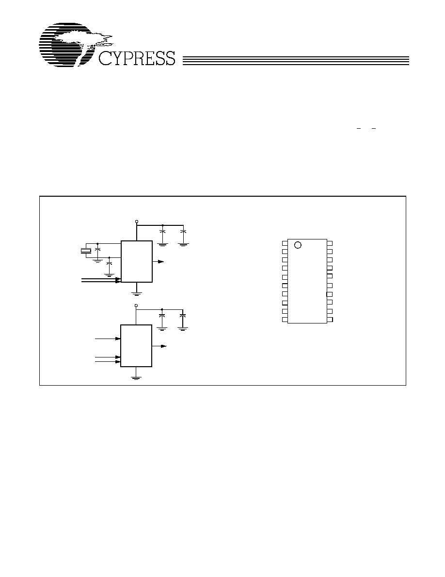
Simplified Block Diagram
Pin Configuration
SSOP
Spread Spectrum
W245-30
(EMI suppressed)
3.3V or 5.0V
Oscillator or
Spread Spectrum
W245-30
(EMI suppressed)
3.3V or 5.0V
XTAL
X1
X2
Reference Input
Input
Output
Output
X1
SCLK
SDATA
SDATA
SCLK
IIC Interface
IIC Interface
SCLK
Notes:
1.
Pins marked with ^ are internal pull-down resistors with
weak 250 k
.
2.
Pins marked with * are internal pull-up resistors with weak
80 k
.
[1, 2]

W245-30
Document #: 38-07229 Rev. *A
Page 2 of 12
Pin Description
Pin Name
Pin No.
Pin
Type
Pin Description
SSOUT
15
O
Output Modulated Frequency: Frequency modulated copy of the input clock
(SSON# asserted).
REFOUT
20
O
Non-Modulated Output: This pin provides a copy of the reference frequency.
This output will not have the Spread Spectrum feature enabled regardless of
the state of logic input SSON#.
X1
1
I
Crystal Connection or External Reference Frequency Input: This pin has
dual functions. It may either be connected to an external crystal, or to an
external reference clock.
X2
2
I
Crystal Connection: Input connection for an external crystal. If using an ex-
ternal reference, this pin must be left unconnected.
SSON#
10
I
Spread Spectrum Control (Active LOW): Asserting this signal (active LOW)
turns the internal modulation waveform on. This pin has an internal pull-down
resistor.
MW0:2
4, 11, 14
I
Modulation Width Selection: When Spread Spectrum feature is turned on,
these pins are used to select the amount of variation and peak EMI reduction
that is desired on the output signal. MW1:Down, MW1:Up, MW2:Down (See
Table 2).
IR1:2
17, 16
I
Reference Frequency Selection: Logic level provided at this input indicates
to the internal logic what range the reference frequency is in and determines
the factor by which the device multiplies the input frequency. Refer to Table 3.
These pins have internal pull-up resistors.
OR1:2
6, 9
I
Output Frequency Selection Bits: These pins select the frequency operation
for the output. Refer to Table 1. OR2 pin have internal pull-up resistors. OR1
pin have internal pull-down resistors.
SCLK
7
I
Clock pin for SMBus circuitry.
SData
5
I/O
Data pin for SMBus Circuitry.
VDD
12, 19
P
Power Connection: Connected to 3.3V or 5V power supply.
AVDD
3
P
Analog Power Connection: Connected to 3.3V or 5V power supply.
GND
8, 13, 18
G
Ground Connection: Connect all ground pins to the common ground plane.
W245-30
Document #: 38-07229 Rev. *A
Page 3 of 12
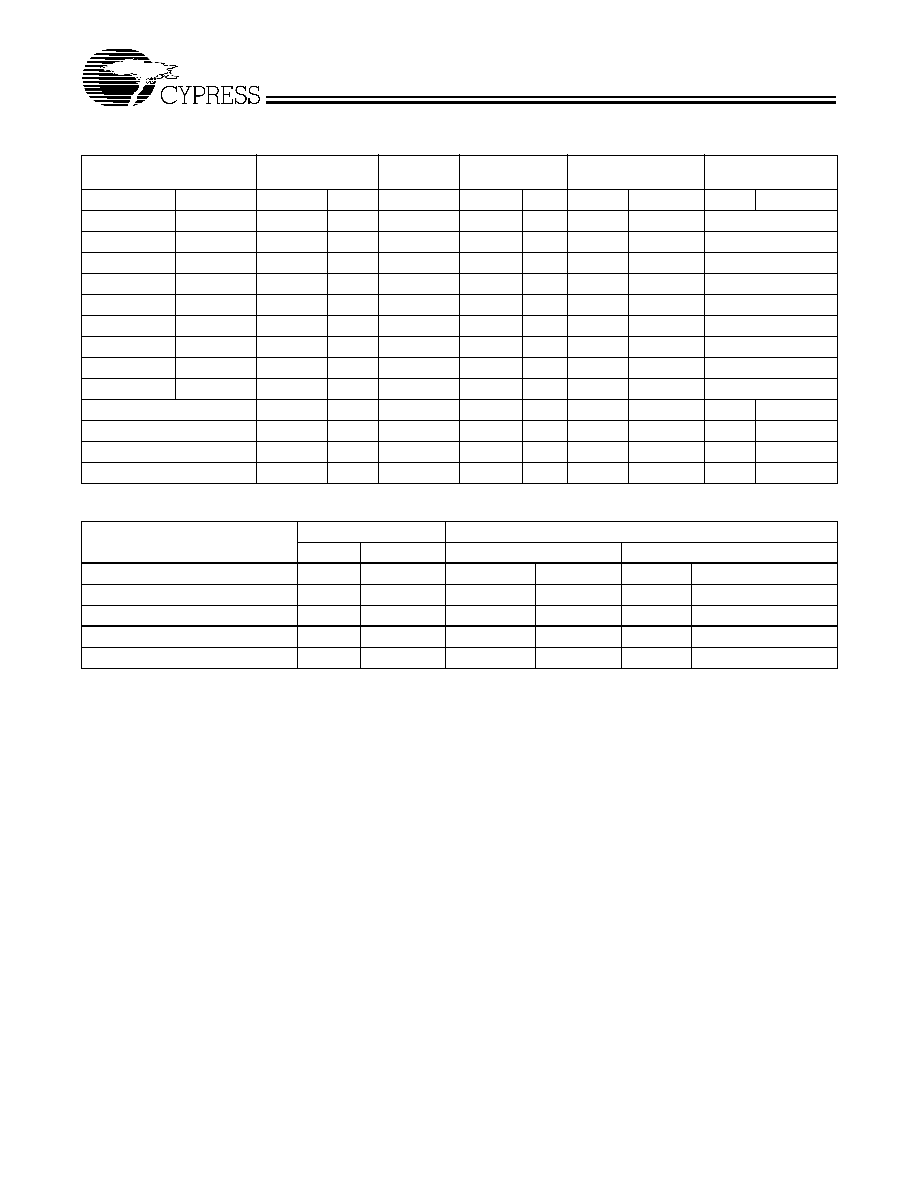
Table 1. Frequency Configuration (Frequencies in MHz)
Table 2. Modulation Width Selection Table
Overview
The W245-30 product is one of a series of devices in the Cy-
press PREMIS family. The PREMIS family incorporates the
latest advances in PLL spread spectrum frequency synthesiz-
er techniques. By frequency modulating the output with a low
frequency carrier, peak EMI is greatly reduced. Use of this
technology allows systems to pass increasingly difficult EMI
testing without resorting to costly shielding or redesign.
In a system, not only is EMI reduced in the various clock lines,
but also in all signals which are synchronized to the clock.
Therefore, the benefits of using this technology increase with
the number of address and data lines in the system. The Sim-
plified Block Diagram shows a simple implementation.
Functional Description
The W245-30 uses a phase locked loop (PLL) to frequency
modulate an input clock. The result is an output clock whose
frequency is slowly swept over a narrow band near the input
signal. The basic circuit topology is shown in Figure 1. The
input reference signal is divided by Q and fed to the phase
detector. A signal from the VCO is divided by P and fed back
to the phase detector also. The PLL will force the frequency of
the VCO output signal to change until the divided output signal
and the divided reference signal match at the phase detector
input. The output frequency is then equal to the ratio of P/Q
times the reference frequency. (Note: For the W245-30 the
output frequency is nominally equal to the input frequency.)
The unique feature of the Spread Spectrum Frequency Timing
Generator is that a modulating waveform is superimposed at
the input to the VCO. This causes the VCO output to be slowly
swept across a predetermined frequency band.
Because the modulating frequency is typically 1000 times
slower than the fundamental clock, the spread spectrum pro-
cess has little impact on system performance.
Frequency Selection With SSFTG
In Spread Spectrum Frequency Timing Generation, EMI re-
duction depends on the shape, modulation percentage, and
frequency of the modulating waveform. While the shape and
frequency of the modulating waveform are fixed for a given
frequency, the modulation percentage may be varied.
Using frequency select bits (FS2:1 pins), the frequency range
can be set (see Table 2). Spreading percentage is set with pins
MW0:2 as shown in Table 2.
A larger spreading percentage improves EMI reduction. How-
ever, large spread percentages may either exceed system
maximum frequency ratings or lower the average frequency to
a point where performance is affected. For these reasons,
spreading percentage options are provided.
Range of Fin
Frequency
Multiplier
Settings
Output /
Input
Range of Fout
Required R
Settings
Modulation & Pow-
er Down Settings
Min.
Max.
OR2
OR1
Min.
Max.
IR2
IR1
MW2
MW1
14
30
0
1
1
14
30
0
1
Table 2
14
30
1
0
2
28
60
0
1
Table 2
14
30
1
1
4
56
120
0
1
Table 2
25
60
0
1
0.5
13
30
1
0
Table 2
25
60
1
0
1
25
60
1
0
Table 2
25
60
1
1
2
50
120
1
0
Table 2
50
120
0
1
0.25
13
30
1
1
Table 2
50
120
1
0
0.5
25
60
1
1
Table 2
50
120
1
1
1
50
120
1
1
Table 2
Reserved
0
0
N/A
N/A
N/A
As Set
As Set
1
0
Power Down Hi-Z
0
0
N/A
N/A
N/A
As Set
As Set
1
1
Power Down 0
0
0
N/A
N/A
N/A
As Set
As Set
0
0
Power Down 1
0
0
N/A
N/A
N/A
As Set
As Set
0
1
EMI Reduction
Modulation Setting
Bandwith Limit Frequencies as a% Value of Fout
MW0 = 0
MW0 = 1
MW2
MW1
Low
High
Low
High
Minimum EMI Control
0
0
98.75%
100%
99.375%
100.625
Suggested Setting
0
1
97.5%
100%
98.75
101.25%
Alternate Setting
1
0
95.0%
100%
97.5%
102.5%
Maximum EMI reduction
1
1
90.0%
100%
95%
105%
W245-30
Document #: 38-07229 Rev. *A
Page 4 of 12
Freq.
Phase
Modulating
VCO
Post
CLKOUT
Detector
Charge
Pump
Waveform
Dividers
Divider
Feedback
Divider
PLL
GND
V
DD
Q
P
Clock Input
Reference Input
(EMI suppressed)
Figure 1. Functional Block Diagram
W245-30
Document #: 38-07229 Rev. *A
Page 5 of 12
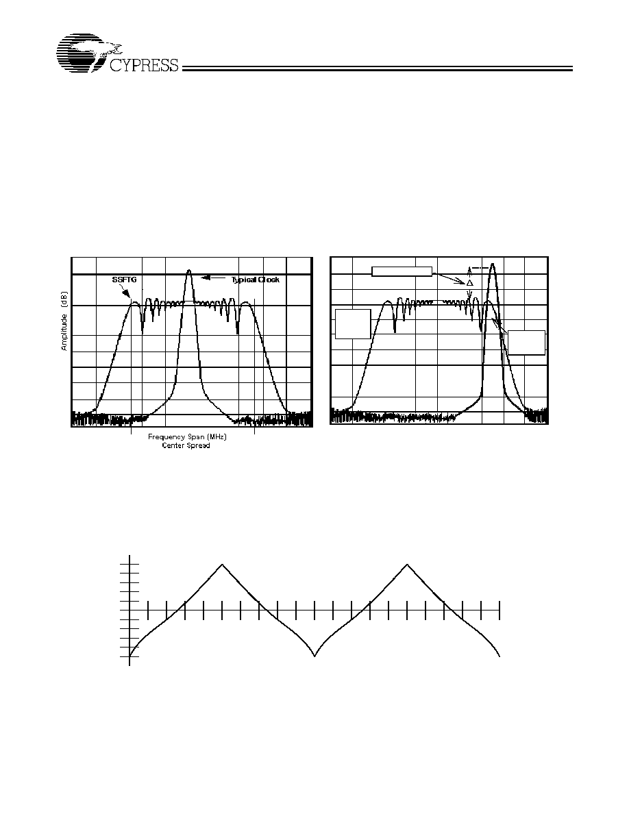
Spread Spectrum Frequency Timing Generator
The device generates a clock that is frequency modulated in
order to increase the bandwidth that it occupies. By increasing
the bandwidth of the fundamental and its harmonics, the am-
plitudes of the radiated electromagnetic emissions are re-
duced. This effect is depicted in Figure 2.
As shown in Figure 2, a harmonic of a modulated clock has a
much lower amplitude than that of an unmodulated signal. The
reduction in amplitude is dependent on the harmonic number
and the frequency deviation or spread. The equation for the
reduction is
dB = 6.5 + 9*log
10
(P) + 9*log
10
(F)
Where P is the percentage of deviation and F is the frequency
in MHz where the reduction is measured.
The output clock is modulated with a waveform depicted in
Figure 3. This waveform, as discussed in "Spread Spectrum
Clock Generation for the Reduction of Radiated Emissions" by
Bush, Fessler, and Hardin produces the maximum reduction
in the amplitude of radiated electromagnetic emissions. The
deviation selected for this chip is as described in Table 2.
Figure 3 details the Cypress spreading pattern. Cypress does
offer options with more spread and greater EMI reduction.
Contact your local Sales representative for details on these
devices.
Spread
Spectrum
Enabled
EMI Reduction
Spread
Spectrum
Non-
Frequency Span (MHz)
Down Spread
A
m
pl
itud
e
(dB
)
Figure 2. Clock Harmonic with and without SSCG Modulation Frequency Domain Representation
MAX.
MIN.
10
%
20
%
30
%
40
%
50
%
60
%
70
%
80
%
90
%
10
0%
10
%
20
%
30
%
40
%
50
%
60
%
70
%
80
%
90
%
10
0%
F
R
EQUENCY
Figure 3. Typical Modulation Profile