 | –≠–ª–µ–∫—Ç—Ä–æ–Ω–Ω—ã–π –∫–æ–º–ø–æ–Ω–µ–Ω—Ç: W250-03H | –°–∫–∞—á–∞—Ç—å:  PDF PDF  ZIP ZIP |
PRELIMINARY
FTG for VIA Apollo Pro-266
W250-03
Cypress Semiconductor Corporation
∑
3901 North First Street
∑
San Jose
∑
CA 95134
∑
408-943-2600
Document #: 38-07254 Rev. *A
Revised December 14, 2002
3
Features
∑ Maximized EMI Suppression using Cypress's Spread
Spectrum Technology
∑ System frequency synthesizer for VIA Apollo Pro-266
∑ Supports IntelÆ PentiumÆ II and PentiumÆ III class pro-
cessor
∑ Three copies of CPU output
∑ Nine copies of PCI output
∑ One 48-MHz output for USB
∑ One 24-MHz or 48-MHz output for SIO
∑ Two buffered reference outputs
∑ Three copies of APIC output
∑ Supports frequencies up to 200 MHz
∑ SMBus interface for programming
∑ Power management control inputs
∑ Available in 48-pin SSOP
Key Specifications
CPU Cycle-to-Cycle Jitter: ................................................ 250 ps
CPU to CPU Output Skew: ............................................... 175 ps
PCI Cycle to Cycle Jitter: .................................................. 500 ps
PCI to PCI Output Skew: .................................................. 500 ps
Intel and Pentium are registered trademarks of Intel Corporation.
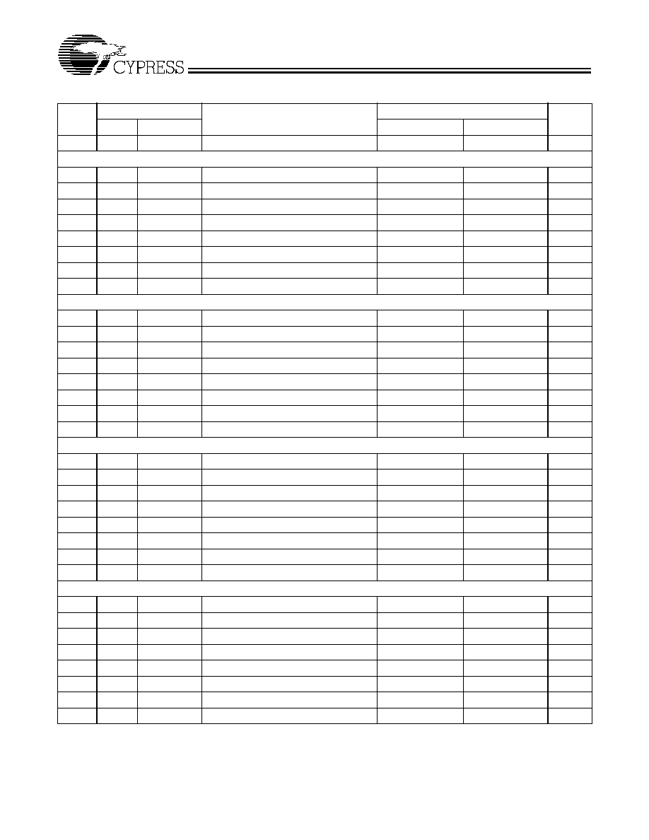
Table 1. Pin Selectable Frequency
Input Address
CPU,
(MHz)
AGP
PCI
(MHz)
Spread
Spectrum
FS4
FS3
FS2
FS1
FS0
0
0
0
0
0
200.0
66.6
33.3
OFF
0
0
0
0
1
190.0
63.3
31.7
OFF
0
0
0
1
0
180.0
60.0
30.0
OFF
0
0
0
1
1
170.0
56.7
28.3
OFF
0
0
1
0
0
166.0
83.0
41.5
OFF
0
0
1
0
1
160.0
80.0
40.0
OFF
0
0
1
1
0
150.0
75.0
37.5
OFF
0
0
1
1
1
145.0
72.5
36.3
OFF
0
1
0
0
0
140.0
70.0
35.0
OFF
0
1
0
0
1
136.0
68.0
34.0
OFF
0
1
0
1
0
130.0
65.0
32.5
OFF
0
1
0
1
1
124.0
62.0
31.0
OFF
0
1
1
0
0
66.6
66.6
33.3
OFF
0
1
1
0
1
100.0
66.6
33.3
OFF
0
1
1
1
0
118.0
78.7
39.3
OFF
0
1
1
1
1
133.3
66.6
33.3
OFF
1
0
0
0
0
66.8
66.8
33.4
+0.25%
1
0
0
0
1
100.2
66.8
33.4
+0.25%
1
0
0
1
0
115.0
76.7
38.3
OFF
1
0
0
1
1
133.6
66.8
33.4
+0.25%
1
0
1
0
0
66.8
66.8
33.4
+0.5%
1
0
1
0
1
100.2
66.8
33.4
+0.5%
1
0
1
1
0
110.0
73.3
36.7
OFF
1
0
1
1
1
133.6
66.8
33.4
+0.5%
1
1
0
0
0
105.0
70.0
35.0
OFF
1
1
0
0
1
90.0
60.0
30.0
OFF
1
1
0
1
0
85.0
56.7
28.3
OFF
1
1
0
1
1
78.0
78.0
39.0
OFF
1
1
1
0
0
66.6
66.6
33.3
-0.5%
1
1
1
0
1
100.0
66.6
33.3
-0.5%
1
1
1
1
0
75.0
75.0
37.5
OFF
1
1
1
1
1
133.3
66.6
33.3 -0.5%
Table 1. Pin Selectable Frequency (continued)
Input Address
CPU,
(MHz)
AGP
PCI
(MHz)
Spread
Spectrum
FS4
FS3
FS2
FS1
FS0
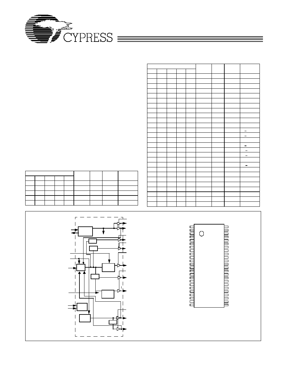
Block Diagram
Pin Configuration
Note:
1.
Signals marked with `*' have internal pull-up resistors.
[1]
VDD_REF
REF0
XTAL
PLL Ref Freq
PLL 1
X2
X1
REF1/FS4
VDD_PCI
Stop
Clock
Control
PCI1:8
48MHz/FS3
24_48MHz/FS2
PLL2
˜2,3,4
OSC
PWR_DWN#
VDD_48 MHz
SMBus
SDATA
Logic
SCLK
CPU1:3
VDD_REF
GND_REF
X1
X2
VDD_48 MHz
FS3*/48 MHz
FS2*/24_48 MHz
GND_48 MHz
PCI_F
PCI1
PCI2
GND_PCI
PCI3
PCI4
VDD_PCI
PCI5
PCI6
PCI7
GND_PCI
PCI8
*FS1
*FS0
AGP0
VDD_AGP
W
2
50-0
3
REF0
REF1/FS4*
VDD_APIC
APIC0
APIC1
GND_APIC
APIC2
VDD_CPU
GND_CPU
CPU1
CPU2
VDD_CPU
GND_CPU
CPU3
CPU_STOP#*
PCI_STOP#*
PWR_DWN#*
VDD_CORE
GND_CORE
SDATA
SCLK
AGP2
AGP1
GND_AGP
48
47
46
45
44
43
42
41
40
39
38
37
36
35
34
33
32
31
30
29
28
27
26
25
1
2
3
4
5
6
7
8
9
10
11
12
13
14
15
16
17
18
19
20
21
22
23
24
˜2
Stop
Clock
Control
PCI_STOP#
PCI_F
DIV
APIC0:2
AGP0:2
DIV
FS0:1
CPU_STOP#
VDD_CPU
VDD_AGP
VDD_APIC
W250-03
PRELIMINARY
Document #: 38-07254 Rev. *A
Page 2 of 12
Pin Definitions
Pin Name
Pin No.
Pin
Type
Pin Description
CPU1:3
39, 38, 35
O
CPU Clock Output: Frequency is set by the FS0:4 input or through serial input interface.
The CPU1:3 output are gated by the CLK_STOP# input.
CPU_STOP#*
34
I
CPU Output Control: 3.3V LVTTL compatible input that stop CPU1:3 clocks.
PCI1:8
10, 11, 13,
14, 16, 17,
18, 20
O
PCI Clock Outputs 1 through 8: Frequency is set by FS0:4 inputs or through serial input
interface, see Table 1 and Table 5 for details. Output voltage swing is controlled by voltage
applied to VDD_PCI.
PCI_STOP#*
33
O
PCI_STOP# Input: 3.3V LVTTL compatible input that stops PCI1:8.
PCI_F
9
O
Free-Running PCI Clock Output: Output voltage swing is controlled by the voltage
applied to VDD_PCI. See Table 1. and Table 5. for detailed frequency information.
PWR_DWN#*
32
I
PWR_DWN# Input: LVTTL-compatible input that places the device in power-down mode
when held LOW.
APIC0:2
45, 44, 42
O
APIC Clock Output: APIC clock outputs. The output voltage swing is controlled by
VDD_APIC.
48MHz/FS3*
6
I/O
48-MHz Output/Frequency Select 3: 48 MHz is provided in normal operation. In stan-
dard PC systems, this output can be used as the reference for the Universal Serial Bus
host controller. This pin also serves as a power-on strap option to determine device
operating frequency as described in Table 1.
24_48MHz/
FS2*
7
I/O
24_48-MHz Output/Frequency Select 2: In standard PC systems, this output can be
used as the clock input for a Super I/O chip. The output frequency is controlled by Con-
figuration Byte 3 bit[6]. The default output frequency is 24 MHz. This pin also serves as
a power-on strap option to determine device operating frequency as described in Table 1.
REF1/FS4*
47
I/O
Reference Clock Output 1/Frequency Select 4: 3.3V 14.318-MHz output clock. This
pin also serves as a power-on strap option to determine device operating frequency as
described in Table 1. Upon power-up, FS4 input will be latched which will set clock fre-
quencies as described in Table 1.
REF0
48
O
Reference Clock Output 0: 3.3V 14.318 MHz output clock.
SCLK
28
I
Clock pin for serial interface circuitry.
SDATA
29
I/O
Data pin for serial interface circuitry.
X1
3
I
Crystal Connection or External Reference Frequency Input: This pin has dual func-
tions. It can be used as an external 14.318-MHz crystal connection or as an external
reference frequency input.
X2
4
I
Crystal Connection: An input connection for an external 14.318-MHz crystal. If using an
external reference, this pin must be left unconnected.
FS0,FS1
22, 21
I
FS0, FS1 Inputs: Latched frequency select inputs. These latched input serve as a power-
on strap option to determine device operating frequency as described in Table 1.
AGP0:2
23, 26, 27
O
AGP Outputs: Output frequency is set by FS0:4 inputs or through serial interface.
VDD_REF,
VDD_48MHz,
VDD_PCI,
VDD_AGP,
VDD_CORE
1, 5,15, 24,
31
P
Power Connection: Power supply for core logic, PLL circuitry, PCI outputs, reference
outputs, 48-MHz output, and 24_48-MHz output, connect to 3.3V supply.
VDD_CPU,
VDD_APIC
41, 46, 37
P
Power Connection: Power supply for APIC and CPU1 output buffers, connect to 2.5V.
GND_REF,
GND_48MHz,
GND_PCI,
GND_AGP,
GND_CORE,
GND_CPU,
GND_APIC
2, 8, 12, 19,
25, 30, 36,
40, 43
G
Ground Connections: Connect all ground pins to the common system ground plane.
W250-03
PRELIMINARY
Document #: 38-07254 Rev. *A
Page 3 of 12
Serial Data Interface
The serial data interface can be used to configure internal reg-
ister settings that control particular device functions. Upon
power-up, the W250-03 initializes with default register set-
tings, therefore the use of this serial data interface is optional.
The serial interface is write-only (to the clock chip) and is the
dedicated function of device pins SDATA and SCLOCK. In
motherboard applications, SDATA and SCLOCK are typically
driven by two logic outputs of the chipset. Clock device register
changes are normally made upon system initialization, if any
are required. The interface can also be used during system
operation for power management functions. Table 2 summa-
rizes the control functions of the serial data interface.
Operation
Data is written to the W250-03 in eleven bytes of eight bits
each. Bytes are written in the order shown in Table 3.
Table 2. Serial Data Interface Control Functions Summary
Control Function
Description
Common Application
Clock Output Disable
Any individual clock output(s) can be disabled. Dis-
abled outputs are actively held LOW.
Unused outputs are disabled to reduce EMI
and system power. Examples are clock out-
puts to unused PCI slots.
CPU Clock Frequency
Selection
Provides CPU/PCI frequency selections through
software. Frequency is changed in a smooth and
controlled fashion.
For alternate microprocessors and power
management options. Smooth frequency
transition allows CPU frequency change un-
der normal system operation.
Spread Spectrum
Enabling
Enables or disables spread spectrum clocking.
For EMI reduction.
Output Three-state
Puts clock output into a high impedance state.
Production PCB testing.
(Reserved)
Reserved function for future device revision or pro-
duction device testing.
No user application. Register bit must be writ-
ten as 0.
Table 3. Byte Writing Sequence
Byte Sequence
Byte Name
Bit Sequence
Byte Description
1
Slave Address
11010010
Commands the W250-03 to accept the bits in Data Bytes 0≠6 for internal
register configuration. Since other devices may exist on the same com-
mon serial data bus, it is necessary to have a specific slave address for
each potential receiver. The slave receiver address for the W250-03 is
11010010. Register setting will not be made if the Slave Address is not
correct (or is for an alternate slave receiver).
2
Command
Code
Don't Care
Unused by the W250-03, therefore bit values are ignored ("don't care").
This byte must be included in the data write sequence to maintain proper
byte allocation. The Command Code Byte is part of the standard serial
communication protocol and may be used when writing to another ad-
dressed slave receiver on the serial data bus.
3
Byte Count
Don't Care
Unused by the W250-03, therefore bit values are ignored ("don't care").
This byte must be included in the data write sequence to maintain proper
byte allocation. The Byte Count Byte is part of the standard serial com-
munication protocol and may be used when writing to another ad-
dressed slave receiver on the serial data bus.
4
Data Byte 0
Refer to Table 4
The data bits in Data Bytes 0≠7 set internal W250-03 registers that
control device operation. The data bits are only accepted when the Ad-
dress Byte bit sequence is 11010010, as noted above. For description
of bit control functions, refer to Table 4, Data Byte Serial Configuration
Map.
5
Data Byte 1
6
Data Byte 2
7
Data Byte 3
8
Data Byte 4
9
Data Byte 5
10
Data Byte 6
11
Data Byte 7
W250-03
PRELIMINARY
Document #: 38-07254 Rev. *A
Page 4 of 12
Writing Data Bytes
Each bit in Data Bytes 0≠7 controls a particular device function
except for the "reserved" bits which must be written as a logic
0. Bits are written MSB (most significant bit) first, which is bit
7. Table 4 gives the bit formats for registers located in Data
Bytes 0≠7.
Table 5 details additional frequency selections that are avail-
able through the serial data interface.
Table 4. Data Bytes 0≠7 Serial Configuration Map
Bit(s)
Affected Pin
Control Function
Bit Control
Default
Pin No.
Pin Name
0
1
Data Byte 0
7
--
--
(Reserved)
--
--
0
6
--
--
SEL_2
See Table 5
0
5
--
--
SEL_1
See Table 5
0
4
--
--
SEL_0
See Table 5
0
3
--
--
Hardware/Software Frequency Select
Hardware
Software
0
2
--
--
SEL_4
See Table 5
1
1
--
--
SEL_3
See Table 5
0
0
--
--
Normal
Three-stated
0
Data Byte 1
7
--
--
(Reserved)
--
--
0
6
--
--
(Reserved)
--
--
0
5
--
--
(Reserved)
--
--
0
4
--
--
(Reserved)
--
--
0
3
35
CPU3
Clock Output Disable
Low
Active
1
2
38
CPU2
Clock Output Disable
Low
Active
1
1
39
CPU1
Clock Output Disable
Low
Active
1
0
42
APIC2
Clock Output Disable
Low
Active
1
Data Byte 2
7
20
PCI8
Clock Output Disable
Low
Active
1
6
18
PCI7
Clock Output Disable
Low
Active
1
5
17
PCI6
Clock Output Disable
Low
Active
1
4
16
PCI5
Clock Output Disable
Low
Active
1
3
14
PCI4
Clock Output Disable
Low
Active
1
2
13
PCI3
Clock Output Disable
Low
Active
1
1
11
PCI2
Clock Output Disable
Low
Active
1
0
10
PCI1
Clock Output Disable
Low
Active
1
Data Byte 3
7
--
--
(Reserved)
--
--
0
6
--
SEL_48MHz
SEL 48MHz as the output frequency for
24_48MHz
24 MHz
48 MHz
0
5
6
48MHz
Clock Output Disable
Low
Active
1
4
7
24_48MHz
Clock Output Disable
Low
Active
1
3
9
PCI_F
Clock Output Disable
Low
Active
1
2
27
AGP2
Clock Output Disable
Low
Active
1
1
26
AGP1
Clock Output Disable
Low
Active
1
W250-03
PRELIMINARY
Document #: 38-07254 Rev. *A
Page 5 of 12
0
23
AGP0
Clock Output Disable
Low
Active
1
Data Byte 4
7
--
--
(Reserved)
--
--
0
6
--
--
(Reserved)
--
--
0
5
--
--
(Reserved)
--
--
0
4
--
--
(Reserved)
--
--
0
3
--
--
(Reserved)
--
--
0
2
--
--
(Reserved)
--
--
0
1
--
--
(Reserved)
--
--
0
0
--
--
(Reserved)
--
--
0
Data Byte 5
7
--
--
(Reserved)
--
--
0
6
--
--
(Reserved)
--
--
0
5
44
APIC1
Clock Output Disable
Low
Active
1
4
45
APIC0
Clock Output Disable
Low
Active
1
3
--
--
(Reserved)
--
--
0
2
--
--
(Reserved)
--
--
0
1
47
REF1
Clock Output Disable
Low
Active
1
0
48
REF0
Clock Output Disable
Low
Active
1
Data Byte 6
7
--
--
(Reserved)
--
--
0
6
--
--
(Reserved)
--
--
0
5
--
--
(Reserved)
--
--
0
4
--
--
(Reserved)
--
--
0
3
--
--
(Reserved)
--
--
0
2
--
--
(Reserved)
--
--
0
1
--
--
(Reserved)
--
--
0
0
--
--
(Reserved)
--
--
0
Data Byte 7
7
--
--
(Reserved)
--
--
0
6
--
--
(Reserved)
--
--
0
5
--
--
(Reserved)
--
--
0
4
--
--
(Reserved)
--
--
0
3
--
--
(Reserved)
--
--
0
2
--
--
(Reserved)
--
--
0
1
--
--
(Reserved)
--
--
0
0
--
--
(Reserved)
--
--
0
Table 4. Data Bytes 0≠7 Serial Configuration Map (continued)
Bit(s)
Affected Pin
Control Function
Bit Control
Default
Pin No.
Pin Name
0
1