 | –≠–ª–µ–∫—Ç—Ä–æ–Ω–Ω—ã–π –∫–æ–º–ø–æ–Ω–µ–Ω—Ç: W256H | –°–∫–∞—á–∞—Ç—å:  PDF PDF  ZIP ZIP |
12 Output Buffer for 2 DDR and 3 SRAM DIMMS
W256
Cypress Semiconductor Corporation
∑
3901 North First Street
∑
San Jose
,
CA 95134
∑
408-943-2600
Document #: 38-07256 Rev. *C
Revised August 30, 2004
Features
∑ One input to 12 output buffer/drivers
∑ Supports up to 2 DDR DIMMs or 3 SDRAM DIMMS
∑ One additional output for feedback
∑ SMBus interface for individual output control
∑ Low skew outputs (< 100 ps)
∑ Supports 266 MHz and 333 MHz DDR SDRAM
∑ Dedicated pin for power management support
∑ Space-saving 28-pin SSOP package
Functional Description
The W256 is a 3.3V/2.5V buffer designed to distribute
high-speed clocks in PC applications. The part has 12 outputs.
Designers can configure these outputs to support 3 unbuffered
standard SDRAM DIMMs and 2 DDR DIMMs. The W256 can
be used in conjunction with the W250-02 or similar clock
synthesizer for the VIA Pro 266 chipset.
The W256 also includes an SMBus interface which can enable
or disable each output clock. On power-up, all output clocks
are enabled (internal pull-up).
Note:
1. Internal 100K pull-up resistors present on inputs marked with *. Design should not rely solely on internal pull-up resistor to set I/O pins HIGH.
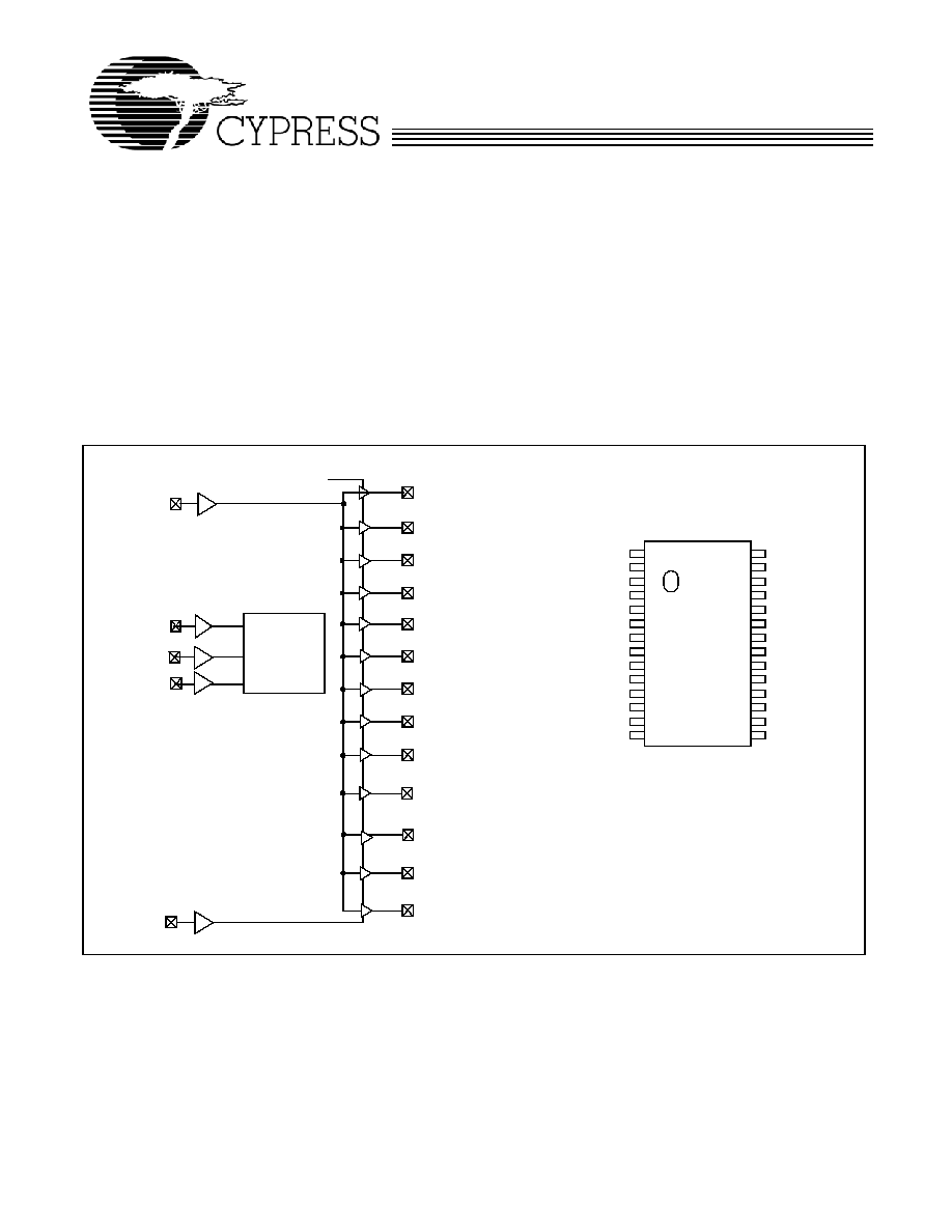
Block Diagram
SMBus
BUF_IN
SDATA
SCLOCK
DDR0T_SDRAM0
DDR0C_SDRAM1
DDR1T_SDRAM2
DDR1C_SDRAM3
SSOP
Top View
Pin Configuration
[1]
Decoding
DDR2T_SDRAM4
DDR2C_SDRAM5
DDR3T_SDRAM6
DDR3C_SDRAM7
DDR4T_SDRAM8
PWR_DWN#
DDR4C_SDRAM9
DDR5T_SDRAM10
DDR5C_SDRAM11
FBOUT
SEL_DDR
FBOUT
*PWR_DWN#
DDR0T_SDRAM0
DDR0C_SDRAM1
VDD3.3_2.5
GND
DDR1T_SDRAM2
DDR1C_SDRAM3
VDD3.3_2.5
BUF_IN
GND
DDR2T_SDRAM4
DDR2C_SDRAM5
VDD3.3_2.5
SEL_DDR*
DDR5T_SDRAM10
DDR5C_SDRAM11
VDD3.3_2.5
GND
DDR4T_SDRAM8
DDR4C_SDRAM9
VDD3.3_2.5
GND
DDR3T_SDRAM6
DDR3C_SDRAM7
GND
SCLK
SDATA
28
27
26
25
24
23
22
21
20
19
18
17
16
15
1
2
3
4
5
6
7
8
9
10
11
12
13
14
&
Powerdown
Control
VDD3.5_2.5

W256
Document #: 38-07256 Rev. *C
Page 2 of 9
Pin Summary
Name
Pins
Description
SEL_DDR
28
Input to configure for DDR-ONLY mode or STANDARD SDRAM mode.
1 = DDR-ONLY mode.
0 = STANDARD SDRAM mode.
When SEL_DDR is pulled HIGH or configured for DDR-ONLY mode, all the buffers
will be configured as DDR outputs.
Connect VDD3.3_2.5 to a 2.5V power supply in DDR-ONLY mode.
When SEL_DDR is pulled LOW or configured for STANDARD SDRAM output, all
the buffers will be configured as STANDARD SDRAM outputs.
Connect VDD3.3_2.5 to a 3.3V power supply in STANDARD SDRAM mode.
SCLK
16
SMBus clock input.
SDATA
15
SMBus data input.
BUF_IN
10
Reference input from chipset. 2.5V input for DDR-ONLY mode; 3.3V input for
STANDARD SDRAM mode.
FBOUT
1
Feedback clock for chipset. Output voltage depends on VDD3.3_2.5V.
PWR_DWN#
2
Active LOW input to enable Power Down mode; all outputs will be pulled LOW.
DDR[0:5]T_SDRAM
[0,2,4,6,8,10]
3, 7, 12, 19, 23, 27
Clock outputs. These outputs provide copies of BUF_IN. Voltage swing depends
on VDD3.3_2.5 power supply.
DDR[0:5]C_SDRAM
[1,3,5,7,9, 11]
4, 8, 13, 18, 22, 26
Clock outputs. These outputs provide complementary copies of BUF_IN when
SEL_DDR is active. These outputs provide copies of BUF_IN when SEL_DDR is
inactive. Voltage swing depends on VDD3.3_2.5 power supply.
VDD3.3_2.5
5, 9, 14, 21, 25
Connect to 2.5V power supply when W256 is configured for DDR-ONLY mode.
Connect to 3.3V power supply, when W256 is configured for standard SDRAM
mode.
GND
6, 11, 17, 20, 24
Ground.
W256
Document #: 38-07256 Rev. *C
Page 3 of 9
Serial Configuration Map
∑ The Serial bits will be read by the clock driver in the following
order:
Byte 0 -- Bits 7, 6, 5, 4, 3, 2, 1, 0
Byte 1 -- Bits 7, 6, 5, 4, 3, 2, 1, 0
.≠
.
Byte N -- Bits 7, 6, 5, 4, 3, 2, 1, 0
∑ Reserved and unused bits should be programmed to "0".
∑ SMBus Address for the W256 is:
Table 1.
A6
A5
A4
A3
A2
A1
A0
R/W
1
1
0
1
0
0
1
≠≠
Byte 6: Outputs Active/Inactive Register
(1 = Active, 0 = Inactive), Default = Active
Bit
Pin #
Description
Default
Bit 7
≠
Reserved, drive to 0
0
Bit 6
≠
Reserved, drive to 0
0
Bit 5
≠
Reserved, drive to 0
0
Bit 4
1
FBOUT
1
Bit 3 27, 26 DDR5T_SDRAM10,
DDR5C_SDRAM11
1
Bit 2
≠
Reserved, drive to 0
1
Bit 1 23, 22 DDR4T_SDRAM8,
DDR4C_SDRAM9
1
Bit 0
≠
Reserved, drive to 0
1
Byte 7: Outputs Active/Inactive Register
(1 = Active, 0 = Inactive), Default = Active
Bit
Pin #
Description
Default
Bit 7
≠
Reserved, drive to 0
1
Bit 6
19, 18
DDR3T_SDRAM6,
DDR3C_SDRAM7
1
Bit 5
12, 13
DDR2T_SDRAM4,
DDR2C_SDRAM5
1
Bit 4
≠
Reserved, drive to 0
1
Bit 3
≠
Reserved, drive to 0
1
Bit 2
7, 8
DDR1T_SDRAM2,
DDR1C_SDRAM3
1
Bit 1
≠
Reserved, drive to 0
1
Bit 0
3, 4
DDR0T_SDRAM0,
DDR0C_SDRAM1
1

W256
Document #: 38-07256 Rev. *C
Page 4 of 9
Maximum Ratings
Supply Voltage to Ground Potential ..................≠0.5 to +7.0V
DC Input Voltage (except BUF_IN) ............ ≠0.5V to V
DD
+0.5
Storage Temperature ..................................≠65∞C to +150∞C
Static Discharge Voltage ............................................>2000V
(per MIL-STD-883, Method 3015)
Operating Conditions
[2]
Parameter
Description
Min.
Typ.
Max.
Unit
V
DD3.3
Supply Voltage
3.135
3.465
V
V
DD2.5
Supply Voltage
2.375
2.625
V
T
A
Operating Temperature (Ambient Temperature)
0
70
∞C
C
OUT
Output Capacitance
6
pF
C
IN
Input Capacitance
5
pF
Electrical Characteristics
Over the Operating Range
Parameter
Description
Test Conditions
Min.
Typ.
Max.
Unit
V
IL
Input LOW Voltage
For all pins except SMBus
0.8
V
V
IH
Input HIGH Voltage
2.0
V
I
IL
Input LOW Current
V
IN
= 0V
50
µ
A
I
IH
Input HIGH Current
V
IN
= V
DD
50
µ
A
I
OH
Output HIGH Current
V
DD
= 2.375V
V
OUT
= 1V
≠18
≠32
mA
I
OL
Output LOW Current
V
DD
= 2.375V
V
OUT
= 1.2V
26
35
mA
V
OL
Output LOW Voltage
[3]
I
OL
= 12 mA, V
DD
= 2.375V
0.6
V
V
OH
Output HIGH Voltage
[3]
I
OH
= ≠12 mA, V
DD
= 2.375V
1.7
V
I
DD
Supply Current
[3]
(DDR-Only mode)
Unloaded outputs, 133 MHz
400
mA
I
DD
Supply Current
(DDR-Only mode)
Loaded outputs, 133 MHz
500
mA
I
DDS
Supply Current
PWR_DWN# = 0
100
µ
A
V
OUT
Output Voltage Swing
See Test Circuity (Refer to
Figure 1)
0.7
V
DD
+ 0.6
V
V
OC
Output Crossing Voltage
(V
DD
/2)
≠0.1
V
DD
/2
(V
DD
/2)
+0.1
V
IN
DC
Input Clock Duty Cycle
48
52
%
Notes:
2. Multiple Supplies: The voltage on any input or I/O pin cannot exceed the power pin during power-up. Power supply sequencing is NOT required.
3. Parameter is guaranteed by design and characterization. Not 100% tested in production.
W256
Document #: 38-07256 Rev. *C
Page 5 of 9
Switching Characteristics
[4]
Parameter
Name
Test Conditions
Min.
Typ.
Max.
Unit
≠
Operating Frequency
66
180
MHz
≠
Duty Cycle
[4,5]
= t
2
˜
t
1
Measured at 1.4V for 3.3V outputs
Measured at VDD/2 for 2.5V outputs.
IN
DC
≠5%
IN
DC
+5%
%
t
3
SDRAM Rising Edge Rate
[4]
Measured between 0.4V and 2.4V
1.0
2.50
V/ns
t
4
SDRAM Falling Edge Rate
[4]
Measured between 2.4V and 0.4V
1.0
2.50
V/ns
t
3d
DDR Rising Edge Rate
[4]
Measured between 20% to 80% of
output (Refer to Figure 1)
0.5
1.50
V/ns
t
4d
DDR Falling Edge Rate
[4]
Measured between 20% to 80% of
output (Refer to Figure 1)
0.5
1.50
V/ns
t
5
Output to Output Skew
[4]
All outputs equally loaded
100
ps
t
6
Output t4o Output Skew for
SDRAM
[2]
All outputs equally loaded
150
ps
t
7
SDRAM Buffer HH Prop. Delay
[4]
Input edge greater than 1 V/ns
5
10
ns
t
8
SDRAM Buffer LLProp. Delay
[4]
Input edge greater than 1 V/ns
5
10
ns
Switching Waveforms
Notes:
4. All parameters specified with loaded outputs.
5. Duty cycle of input clock is 50%. Rising and falling edge rate is greater than 1V/ns.
Duty Cycle Timing
t
1
t
2
All Outputs Rise/Fall Time
OUTPUT
t
3
3.3V
0V
0.4V
2.4V
2.4V
0.4V
t
4
Output-Output Skew
t
5
OUTPUT
OUTPUT