 | –≠–ª–µ–∫—Ç—Ä–æ–Ω–Ω—ã–π –∫–æ–º–ø–æ–Ω–µ–Ω—Ç: W311H | –°–∫–∞—á–∞—Ç—å:  PDF PDF  ZIP ZIP |

Preliminary
FTG for VIA Pro-266 DDR Chipset
W311
Cypress Semiconductor Corporation
∑
3901 North First Street
∑
San Jose
∑
CA 95134
∑
408-943-2600
March 15, 2001
1W311
Features
∑ Maximized EMI Suppression using Cypress's Spread
Spectrum Technology
∑ System frequency synthesizer for VIA Pro-2000
∑ Programmable clock output frequency with less than
1 MHz increment
∑ Integrated fail-safe Watchdog Timer for system
recovery
∑ Automatically switch to HW selected or SW
programmed clock frequency when Watchdog Timer
time-out
∑ Capable of generate system RESET after a Watchdog
Timer time-out occurs or a change in output frequency
via SMBus interface
∑ Support SMBus byte read/write and block read/ write
operations to simplify system BIOS development
∑ Vendor ID and Revision ID support
∑ Programmable drive strength for CPU and PCI output
clocks
∑ Programmable output skew between CPU, AGP and PCI
∑ Supports IntelÆ CeleronÆ and PentiumÆ III class pro-
cessor
∑ Three copies of CPU output
∑ Nine copies of PCI output
∑ One 48-MHz output for USB
∑ One 24-MHz or 48-MHz output for SIO
∑ Two buffered reference outputs
∑ Three copies of APIC output
∑ Supports frequencies up to 200 MHz
∑ SMBus interface for programming
∑ Power management control inputs
∑ Available in 48-pin SSOP
Key Specifications
CPU Cycle-to-Cycle Jitter:........................................... 250 ps
CPU to CPU Output Skew: .......................................... 175 ps
PCI Cycle to Cycle Jitter:............................................. 500 ps
PCI to PCI Output Skew: ............................................. 500 ps
Intel, Pentium, and Celeron are registered trademarks of Intel Corporation.
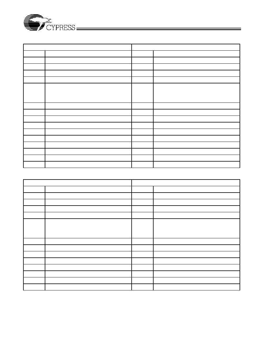
Block Diagram
Pin Configuration
Note:
1.
Signals marked with `*' have internal pull-up resistors.
[1]
V D D _ R E F
R E F 0
XTA L
PLL Ref Freq
PLL 1
X 2
X 1
R E F 1 /F S 4
V D D _ P C I
Stop
Clock
C ontrol
P C I1 :8
4 8 M H z/F S 3
2 4 _ 4 8 M H z/F S 2
PLL2
˜6, ˜8,
OSC
PW R _ D W N #
V D D _ 4 8 M H z
SM Bus
SD ATA
Logic
S C L K
C P U 1 :3
R S T #
VDD_REF
GND_REF
X1
X2
VDD_48 MHz
FS3*/48 MHz
FS2*/24_48 MHz
GND_48 MHz
PCI_F
PCI1
PCI2
GND_PCI
PCI3
PCI4
VDD_PCI
PCI5
PCI6
PCI7
GND_PCI
PCI8
*FS1
*FS0
AGP0
VDD_AGP
W3
1
1
REF0
REF1/FS4*
VDD_APIC
APIC0
APIC1
GND_APIC
APIC2
VDD_CPU
GND_CPU
CPU1
CPU2
VDD_CPU
GND_CPU
CPU3
CPU_STOP#*
PCI_STOP#*
RST#
VDD_CORE
GND_CORE
SDATA
SCLK
AGP2
AGP1
GND_AGP
48
47
46
45
44
43
42
41
40
39
38
37
36
35
34
33
32
31
30
29
28
27
26
25
1
2
3
4
5
6
7
8
9
10
11
12
13
14
15
16
17
18
19
20
21
22
23
24
˜2
Stop
C lock
C ontrol
P C I_ STO P #
P C I_ F
DIV
A P IC 0 :1
A G P 0:2
DIV
FS 0:1
C P U _ STO P #
V D D _C P U
V D D _ A G P
V D D _ A P IC
˜10, ˜12

W311
Preliminary
2
Pin Definitions
Pin Name
Pin No.
Pin
Type
Pin Description
RST#
32
O
(open-
drain)
System Reset Output: Open-drain system reset output.
CPU1:3
39, 38, 35
O
CPU Clock Output: Frequency is set by the FS0:4 input or through serial input interface.
The CPU1:3 outputs are gated by the CLK_STOP# input.
CPU_STOP#
34
I
CPU Output Control: 3.3V LVTTL-compatible input that stop CPU1:3.
PCI1:8
10, 11, 13,
14, 16, 17,
18, 20
O
PCI Clock Outputs 1 through 8: Frequency is set by FS0:4 inputs or through serial
input interface; see Table 5 for details. PCI1:8 outputs are gated by the PCI_STOP#
input.
PCI_STOP#
33
O
PCI_STOP# Input: 3.3V LVTTL-compatible input that stops PCI1:8.
PCI_F
9
O
Free-Running PCI Clock Output: Frequency is set by FS0:4 inputs or through serial
input interface; see Table 5 for details.
APIC0:2
45, 44, 42
O
APIC Clock Output: APIC clock outputs.
48MHz/FS3
6
I/O
48-MHz Output/Frequency Select 3: 48 MHz is provided in normal operation. In stan-
dard PC systems, this output can be used as the reference for the Universal Serial Bus
host controller. This pin also serves as a power-on strap option to determine device
operating frequency as described in Table 5.
24_48MHz/
FS2
7
I/O
24_48-MHz Output/Frequency Select 2: In standard PC systems, this output can be
used as the clock input for a Super I/O chip. The output frequency is controlled by
Configuration Byte 3 bit[6]. The default output frequency is 24 MHz. This pin also serves
as a power-on strap option to determine device operating frequency as described in
Table 5.
REF1/FS4
47
I/O
Reference Clock Output 1/Frequency Select 4: 3.3V 14.318-MHz output clock. This
pin also serves as a power-on strap option to determine device operating frequency as
described in Table 5.
REF0
48
O
Reference Clock Output 0: 3.3V 14.318-MHz output clock.
SCLK
28
I
Clock pin for SMBus circuitry.
SDATA
29
I/O
Data pin for SMBus circuitry.
X1
3
I
Crystal Connection or External Reference Frequency Input: This pin has dual func-
tions. It can be used as an external 14.318-MHz crystal connection or as an external
reference frequency input.
X2
4
I
Crystal Connection: An input connection for an external 14.318-MHz crystal. If using
an external reference, this pin must be left unconnected.
VDD_REF,
VDD_48MHz,
VDD_PCI,
VDD_AGP,
VDD_CORE
1, 5,15, 24,
31
P
Power Connection: Power supply for core logic, PLL circuitry, PCI outputs, reference
outputs, 48-MHz output, and 24_48-MHz output, connect to 3.3V supply.
VDD_CPU,
VDD_APIC
41, 46, 37
P
Power Connection: Power supply for APIC and CPU output buffers, connect to 2.5V.
GND_REF,
GND_48MHz,
GND_PCI,
GND_AGP,
GND_CORE,
GND_CPU,
GND_APIC
2, 8, 12, 19,
25, 30, 36,
40, 43
G
Ground Connections: Connect all ground pins to the common system ground plane.

W311
Preliminary
3
Serial Data Interface
The W312 features a two-pin, serial data interface that can be
used to configure internal register settings that control partic-
ular device functions.
Data Protocol
The clock driver serial protocol supports byte/word write,
byte/word read, block write, and block read operations from the
controller. For block write/read operation, the bytes must be
accessed in sequential order from lowest to highest byte with
the ability to stop after any complete byte has been transferred.
For byte/word write and byte read operations, system control-
ler can access individual indexed byte. The offset of the in-
dexed byte is encoded in the command code.
The definition for the command code is defined as follows:
Table 1. Command Code Definition
Bit
Descriptions
7
0 = Block read or block write operation
1 = Byte/Word read or byte/word write operation
6:0
Byte offset for byte/word read or write operation. For block read or write operations, these bits
need to be set at `0000000'.
Table 2. Block Read and Block Write Protocol
Block Write Protocol
Block Read Protocol
Bit
Description
Bit
Description
1
Start
1
Start
2:8
Slave address - 7 bits
2:8
Slave address - 7 bits
9
Write
9
Write
10
Acknowledge from slave
10
Acknowledge from slave
11:18
Command Code - 8 bits
`00000000' stands for block operation
11:18
Command Code - 8 bits
`00000000' stands for block operation
19
Acknowledge from slave
19
Acknowledge from slave
20:27
Byte Count - 8 bits
20
Repeat start
28
Acknowledge from slave
21:27
Slave address - 7 bits
29:36
Data byte 0 - 8 bits
28
Read
37
Acknowledge from slave
29
Acknowledge from slave
38:45
Data byte 1 - 8 bits
30:37
Byte count from slave - 8 bits
46
Acknowledge from slave
38
Acknowledge
...
Data Byte N/Slave Acknowledge...
39:46
Data byte from slave - 8 bits
...
Data Byte N - 8 bits
47
Acknowledge
...
Acknowledge from slave
48:55
Data byte from slave - 8 bits
...
Stop
56
Acknowledge
...
Data bytes from slave/Acknowledge
...
Data byte N from slave - 8 bits
...
Not Acknowledge
...
Stop
W311
Preliminary
4
Table 3. Word Read and Word Write Protocol
Word Write Protocol
Word Read Protocol
Bit
Description
Bit
Description
1
Start
1
Start
2:8
Slave address - 7 bits
2:8
Slave address - 7 bits
9
Write
9
Write
10
Acknowledge from slave
10
Acknowledge from slave
11:18
Command Code - 8 bits
`1xxxxxxx' stands for byte or word operation
bit[6:0] of the command code represents the off-
set of the byte to be accessed
11:18
Command Code - 8 bits
`1xxxxxxx' stands for byte or word operation
bit[6:0] of the command code represents the off-
set of the byte to be accessed
19
Acknowledge from slave
19
Acknowledge from slave
20:27
Data byte low- 8 bits
20
Repeat start
28
Acknowledge from slave
21:27
Slave address - 7 bits
29:36
Data byte high - 8 bits
28
Read
37
Acknowledge from slave
29
Acknowledge from slave
38
Stop
30:37
Data byte low from slave - 8 bits
38
Acknowledge
39:46
Data byte high from slave - 8 bits
47
NOT acknowledge
48
Stop
Table 4. Byte Read and Byte Write Protocol
Byte Write Protocol
Byte Read Protocol
Bit
Description
Bit
Description
1
Start
1
Start
2:8
Slave address - 7 bits
2:8
Slave address - 7 bits
9
Write
9
Write
10
Acknowledge from slave
10
Acknowledge from slave
11:18
Command Code - 8 bits
`1xxxxxxx' stands for byte operation
bit[6:0] of the command code represents the off-
set of the byte to be accessed
11:18
Command Code - 8 bits
`1xxxxxxx' stands for byte operation
bit[6:0] of the command code represents the off-
set of the byte to be accessed
19
Acknowledge from slave
19
Acknowledge from slave
20:27
Data byte - 8 bits
20
Repeat start
28
Acknowledge from slave
21:27
Slave address - 7 bits
29
Stop
28
Read
29
Acknowledge from slave
30:37
Data byte from slave - 8 bits
38
Not Acknowledge
39
Stop
W311
Preliminary
5
W311 Serial Configuration Map
1. The serial bits will be read by the clock driver in the following
order:
Byte 0 - Bits 7, 6, 5, 4, 3, 2, 1, 0
Byte 1 - Bits 7, 6, 5, 4, 3, 2, 1, 0
Byte N - Bits 7, 6, 5, 4, 3, 2, 1, 0
2. All unused register bits (reserved and N/A) should be writ-
ten to a "0" level.
3. All register bits labeled "Initialize to 0" must be written to
zero during initialization.
Byte 0: Control Register 0
Bit
Pin#
Name
Default
Description
Bit 7
-
Reserved
0
Reserved
Bit 6
-
SEL2
0
See Table 5
Bit 5
-
SEL1
0
See Table 5
Bit 4
-
SEL0
0
See Table 5
Bit 3
-
FS_Override
0
0 = Select operating frequency by FS[4:0] input pins
1 = Select operating frequency by SEL[4:0] settings
Bit 2
-
SEL4
1
See Table 5
Bit 1
-
SEL3
0
See Table 5
Bit 0
-
Reserved
0
Reserved
Byte 1: Control Register 1
Bit
Pin#
Name
Default
Description
Bit 7
-
Reserved
0
Reserved
Bit 6
-
Spread Select2
0
`000' = Normal (spread off)
`001' = Test Mode
`010' = Reserved
`011' = Three-Stated
`100' = ≠0.5%
`101' = ± 0.5%
`110' = ± 0.25%
`111' = ± 0.38%
Bit 5
-
Spread Select1
0
Bit 4
-
Spread Select0
0
Bit 3
35
CPU3
1
(Active/Inactive)
Bit 2
38
CPU2
1
(Active/Inactive)
Bit 1
39
CPU1
1
(Active/Inactive)
Bit 0
42
APIC2
1
(Active/Inactive)
Byte 2: Control Register 2
Bit
Pin#
Name
Default
Description
Bit 7
20
PCI8
1
(Active/Inactive)
Bit 6
18
PCI7
1
(Active/Inactive)
Bit 5
17
PCI6
1
(Active/Inactive)
Bit 4
16
PCI5
1
(Active/Inactive)
Bit 3
14
PCI4
1
(Active/Inactive)
Bit 2
13
PCI3
1
(Active/Inactive)
Bit 1
11
PCI2
1
(Active/Inactive)