SDRAM Buffer - 2 DIMM (Mobile)
W40S11-02
Cypress Semiconductor Corporation
∑
3901 North First Street
∑
San Jose
∑
CA 95134
∑
408-943-2600
September 29, 1999, rev. **
Features
∑ Ten skew-controlled CMOS outputs (SDRAM0:9)
∑ Supports two SDRAM DIMMs
∑ Ideal for high-performance systems designed around
Intelģ's latest Mobile chip set
∑ I
2
C Serial configuration interface
∑ Skew between any two outputs is less than 250 ps
∑ 1 to 5 ns propagation delay
∑ DC to 133-MHz operation
∑ Single 3.3V supply voltage
∑ Low power CMOS design packaged in a 28-pin, 209-mil
SSOP (Shrink Small Outline Package)
Overview
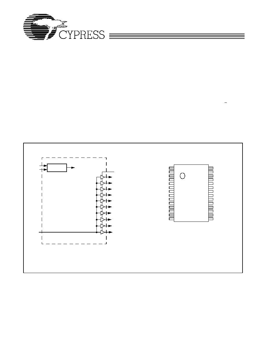
The Cypress W40S11-02 is a low-voltage, ten-output clock
buffer. Output buffer impedance is approximately 15
, which
is ideal for driving SDRAM DIMMs.
Key Specifications
Supply Voltages:........................................... V
DD
= 3.3VĪ5%
Operating Temperature:.................................... 0įC to +70įC
Input Threshold: .................................................. 1.5V typical
Maximum Input Voltage: .......................................V
DD
+ 0.5V
Input Frequency:............................................... 0 to 133 MHz
BUF_IN to SDRAM0:9 Propagation Delay: ........1.0 to 5.0 ns
Output Edge Rate:................................................. >1.5 V/ns
Output Skew: ............................................................ Ī250 ps
Output Duty Cycle: .................................. 45/55% worst case
Output Impedance: ........................................15 ohms typical
Output Type: ................................................ CMOS rail-to-rail
Intel is a registered trademark of Intel Corporation.
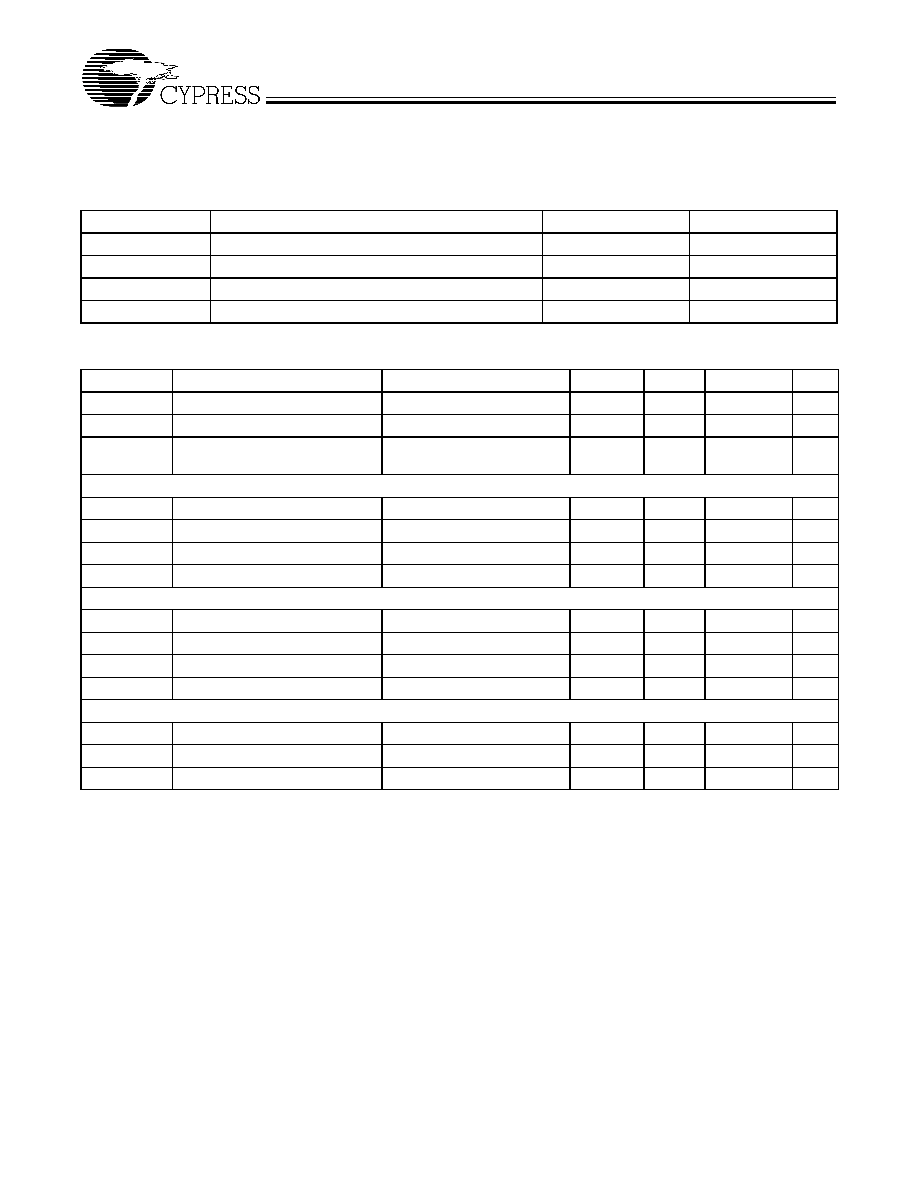
Pin Configuration
Block Diagram
Note:
1.
Internal pull-up resistor of 250K on SDATA, SCLOCK, and OE
inputs (should not be relied upon for pulling up to V
DD
).
[1]
[1]
SDRAM1
SDRAM2
SDRAM3
SDRAM4
SDRAM5
SDRAM6
SDRAM7
SDRAM8
SDRAM9
SDRAM0
Serial Port
SCLOCK
SDATA
Device Control
BUF_IN
OE
VDD
SDRAM0
SDRAM1
GND
VDD
SDRAM2
SDRAM3
GND
BUF_IN
VDD
SDRAM8
GND
VDD
SDATA
VDD
SDRAM7
SDRAM6
GND
VDD
SDRAM5
SDRAM4
GND
OE
VDD
SDRAM9
GND
GND
SCLOCK
28
27
26
25
24
23
22
21
20
19
18
17
16
15
1
2
3
4
5
6
7
8
9
10
11
12
13
14
[1]

W40S11-02
2
Pin Definitions
Pin Name
Pin
No.
Pin
Type
Pin Description
SDRAM0:9
2, 3, 6, 7,
22, 23, 26,
27, 11, 18
O
SDRAM Outputs: Provides buffered copy of BUF_IN. The propagation delay from a
rising input edge to a rising output edge is 1 to 5 ns. All outputs are skew controlled
to within Ī 250 ps of each other.
BUF_IN
9
I
Clock Input: This clock input has an input threshold voltage of 1.5V (typ).
SDATA
14
I/O
I
2
C Data Input: Data should be presented to this input as described in the I
2
C section
of this data sheet. Internal 250-k
pull-up resistor.
SCLOCK
15
I
I
2
C Clock Input: The I
2
C Data clock should be presented to this input as described
in the I
2
C section of this data sheet. Internal 250-k
pull-up resistor.
VDD
1, 5, 10, 13,
19, 24, 28
P
Power Connection: Power supply for core logic and output buffers. Connected to
3.3V supply.
GND
4, 8, 12, 16,
17, 21, 25
G
Ground Connection: Connect all ground pins to the common system ground plane.
OE
20
I
Output Enable: Internal 250-k
pull-up resistor. Three-states outputs when LOW.

W40S11-02
3
Functional Description
Output Control Pins
Outputs three-stated when OE = 0, and toggle when OE = 1.
Outputs are in phase with BUF_IN but are phase delayed by 1
to 5 ns. Outputs can also be controlled via the I
2
C interface.
Output Drivers
The W40S11-02 output buffers are CMOS type which deliver
a rail-to-rail (GND to V
DD
) output voltage swing into a nominal
capacitive load. Thus, output signaling is both TTL and CMOS
level compatible. Nominal output buffer impedance is 15 ohms.
Operation
Data is written to the W40S11-02 in ten bytes of eight bits
each. Bytes are written in the order shown in Table 1.
Table 1. Byte Writing Sequence
Byte
Sequence
Byte Name
Bit Sequence
Byte Description
1
Slave Address
11010010
Commands the W40S11-02 to accept the bits in Data Bytes 0≠6 for in-
ternal register configuration. Since other devices may exist on the same
common serial data bus, it is necessary to have a specific slave address
for each potential receiver. The slave receiver address for the W40S11-02
is 11010010. Register setting will not be made if the Slave Address is not
correct (or is for an alternate slave receiver).
2
Command
Code
Don't Care
Unused by the W40S11-02, therefore bit values are ignored (don't care).
This byte must be included in the data write sequence to maintain proper
byte allocation. The Command Code Byte is part of the standard serial
communication protocol and may be used when writing to another ad-
dressed slave receiver on the serial data bus.
3
Byte Count
Don't Care
Unused by the W40S11-02, therefore bit values are ignored (don't care).
This byte must be included in the data write sequence to maintain proper
byte allocation. The Byte Count Byte is part of the standard serial com-
munication protocol and may be used when writing to another addressed
slave receiver on the serial data bus.
4
Data Byte 0
Refer to Table 2
The data bits in these bytes set internal W40S11-23 registers that control
device operation. The data bits are only accepted when the Address Byte
bit sequence is 11010010, as noted above. For description of bit control
functions, refer to Table 2, Data Byte Serial Configuration Map.
5
Data Byte 1
6
Data Byte 2
7
Data Byte 3
Don't Care
Refer to Cypress clock drivers.
8
Data Byte 4
9
Data Byte 5
10
Data Byte 6
W40S11-02
4
Writing Data Bytes
Each bit in the data bytes control a particular device function.
Bits are written MSB (most significant bit) first, which is bit 7.
Table 2 gives the bit formats for registers located in Data Bytes
0≠6.
Note:
2.
At power-up all SDRAM outputs are enabled and active. It is recommended to program Bits 4≠7 of Byte0 and Bits 0≠3 of Byte1 to a "0" to save power and reduce
noise.
Table 2. Data Bytes 0≠2 Serial Configuration Map
[2]
Bit(s)
Affected Pin
Control Function
Bit Control
Pin No.
Pin Name
0
1
Data Byte 0 SDRAM Active/Inactive Register (1=Enable, 0=Disable)
7
N/A
Reserved
(Reserved)
--
--
6
N/A
Reserved
(Reserved)
--
--
5
N/A
Reserved
(Reserved)
--
--
4
N/A
Reserved
(Reserved)
--
--
3
7
SDRAM3
Clock Output Disable
Low
Active
2
6
SDRAM2
Clock Output Disable
Low
Active
1
3
SDRAM1
Clock Output Disable
Low
Active
0
2
SDRAM0
Clock Output Disable
Low
Active
Data Byte 1 SDRAM Active/Inactive Register (1=Enable, 0=Disable)
7
27
SDRAM7
Clock Output Disable
Low
Active
6
26
SDRAM6
Clock Output Disable
Low
Active
5
23
SDRAM5
Clock Output Disable
Low
Active
4
22
SDRAM4
Clock Output Disable
Low
Active
3
N/A
Reserved
(Reserved)
--
--
2
N/A
Reserved
(Reserved)
--
--
1
N/A
Reserved
(Reserved)
--
--
0
N/A
Reserved
(Reserved)
--
--
Data Byte 2 SDRAM Active/Inactive Register (1=Enable, 0=Disable)
7
18
SDRAM9
Clock Output Disable
Low
Active
6
11
SDRAM8
Clock Output Disable
Low
Active
5
N/A
Reserved
(Reserved)
--
--
4
N/A
Reserved
(Reserved)
--
--
3
N/A
Reserved
(Reserved)
--
--
2
N/A
Reserved
(Reserved)
--
--
1
N/A
Reserved
(Reserved)
--
--
0
N/A
Reserved
(Reserved)
--
--
W40S11-02
5
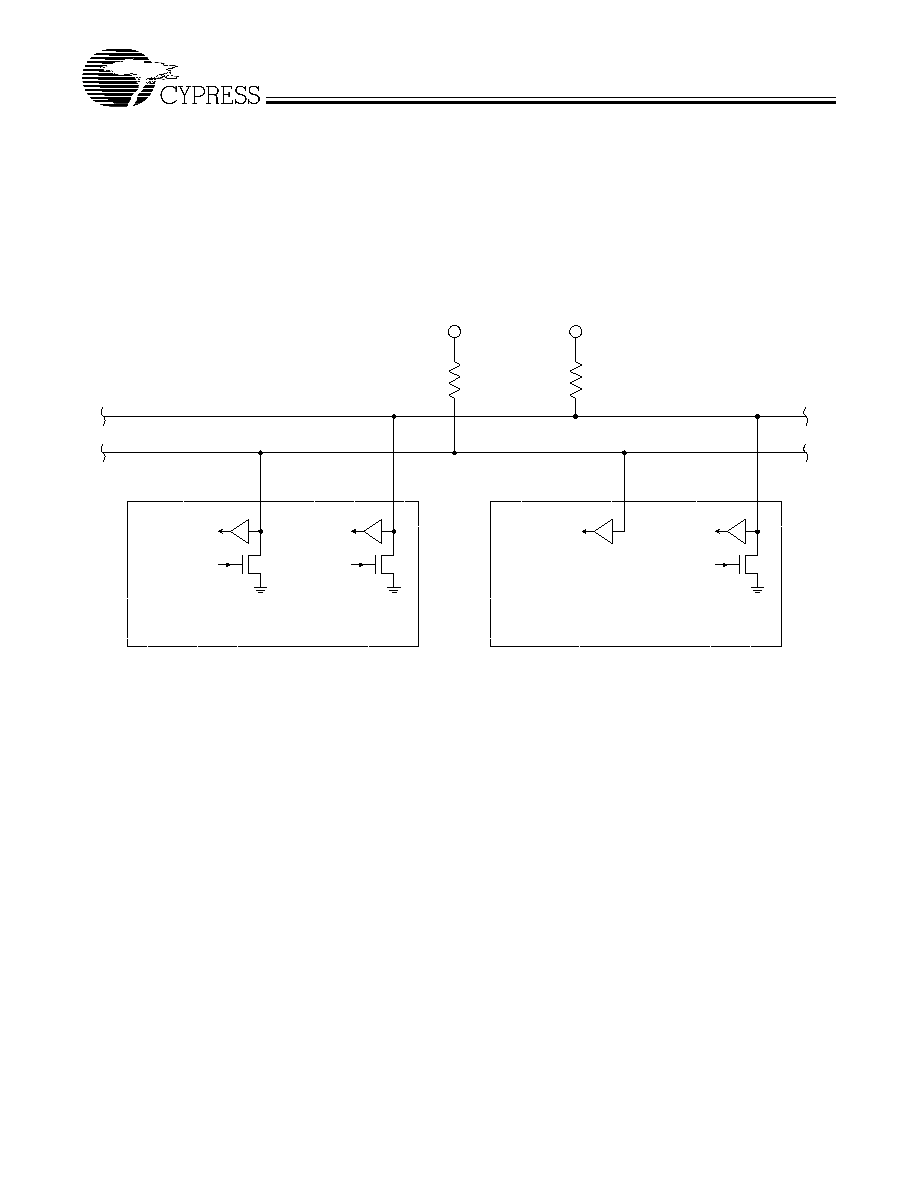
How To Use the Serial Data Interface
Electrical Requirements
Figure 1 illustrates electrical characteristics for the serial inter-
face bus used with the W40S11-02. Devices send data over
the bus with an open drain logic output that can (a) pull the bus
line LOW, or (b) let the bus default to logic 1. The pull-up resis-
tor on the bus (both clock and data lines) establish a default
logic 1. All bus devices generally have logic inputs to receive
data.
Although the W40S11-02 is a receive-only device (no data
write-back capability), it does transmit an "acknowledge" data
pulse after each byte is received. Thus, the SDATA line can
both transmit and receive data.
The pull-up resistor should be sized to meet the rise and fall
times specified in AC parameters, taking into consideration to-
tal bus line capacitance.
DATA IN
DATA OUT
N
CLOCK IN
C L O C K O U T
CHIP SET
(SERIAL BUS MASTER TRANSMITTER)
S D C L K
SDATA
SERIAL BUS CLOCK LINE
SERIAL BUS DATA LINE
N
DATA IN
DATA OUT
CLOCK IN
C L O C K D E V I C E
(SERIAL BUS SLAVE RECEIVER)
S C L O C K
SDATA
N
~ 2k
~ 2k
V D D
V D D
Figure 1. Serial Interface Bus Electrical Characteristics
W40S11-02
6
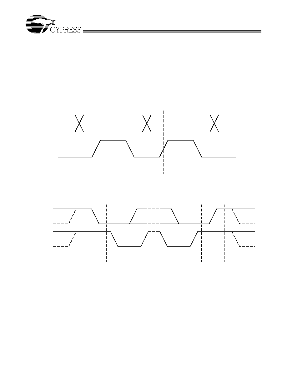
Signaling Requirements
As shown in Figure 2, valid data bits are defined as stable logic
0 or 1 condition on the data line during a clock HIGH (logic 1)
pulse. A transitioning data line during a clock HIGH pulse may
be interpreted as a start or stop pulse (it will be interpreted as
a start or stop pulse if the start/stop timing parameters are
met).
A write sequence is initiated by a "start bit" as shown in Figure
3. A "stop bit" signifies that a transmission has ended.
As stated previously, the W40S11-02 sends an "acknowledge"
pulse after receiving eight data bits in each byte as shown in
Figure 4.
Sending Data to the W40S11-02
The device accepts data once it has detected a valid start bit
and address byte sequence. Device functionality is changed
upon the receipt of each data bit (registers are not double buff-
ered). Partial transmission is allowed meaning that a transmis-
sion can be truncated as soon as the desired data bits are
transmitted (remaining registers will be unmodified). Transmis-
sion is truncated with either a stop bit or new start bit (restart
condition).
SDATA
S C L O C K
Valid
Data
Bit
Change
of Data Allowed
Figure 2. Serial Data Bus Valid Data Bit
S D A T A
S C L O C K
Start
Bit
Stop
Bit
Figure 3. Serial Data Bus Start and Stop Bit

W
4
0S
11
-0
2
7
MSB
1
2
3
4
5
6
7
8
A
1
2
3
4
5
6
7
8
A
1
2
3
4
SCLOCK
1
2
3
4
5
6
7
8
A
1
1
0
1
0
0
1
0
LSB
MSB
MSB
LSB
SDATA
SDATA
Signaling from System Core Logic
Start Condition
MSB
LSB
Slave Address
(First Byte)
Command Code
(Second Byte)
Last Data Byte
(Last Byte)
Byte Count
(Third Byte)
Stop Condition
Signaling by Clock Device
Acknowledgment Bit
from Clock Device
Fi
gur
e 4.
Seri
al
Dat
a
Bus
W
r
i
t
e S
e
quence
t
STHD
t
LOW
t
R
t
HIGH
t
F
t
DSU
t
DHD
t
SP
t
SPSU
t
STHD
t
SPSU
t
SPF
SDATA
SCLOCK
Fi
gur
e 5.
Se
r
i
al
Dat
a
Bus
Ti
m
i
ng Di
agr
a
m
W40S11-02
8
Absolute Maximum Ratings
Stresses greater than those listed in this table may cause per-
manent damage to the device. These represent a stress rating
only. Operation of the device at these or any other conditions
above those specified in the operating sections of this specifi-
cation is not implied. Maximum conditions for extended peri-
ods may affect reliability.
Parameter
Description
Rating
Unit
V
DD
, V
IN
Voltage on any pin with respect to GND
≠0.5 to +7.0
V
T
STG
Storage Temperature
≠65 to +150
įC
T
A
Operating Temperature
0 to +70
įC
T
B
Ambient Temperature under Bias
≠55 to +125
įC
DC Electrical Characteristics:
T
A
= 0įC to +70įC, V
DD
= 3.3VĪ5%
Parameter
Description
Test Condition/Comments
Min
Typ
Max
Unit
I
DD
3.3V Supply Current
at 66 MHz
120
160
mA
I
DD
3.3V Supply Current
at 100 MHz
185
220
mA
I
DD Tristate
3.3V Supply Current in
Three-State
5
10
mA
Logic Inputs
V
IL
Input Low Voltage
V
SS
≠0.3
0.8
V
V
IH
Input High Voltage
2.0
V
DD
+0.5
V
I
ILEAK
Input Leakage Current, BUF_IN
≠5
+5
ĶA
I
ILEAK
Input Leakage Current
[3]
≠20
+5
ĶA
Logic Outputs (SDRAM0:9)
[4]
V
OL
Output Low Voltage
I
OL
= 1 mA
50
mV
V
OH
Output High Voltage
I
OH
= ≠1 mA
3.1
V
I
OL
Output Low Current
V
OL
= 1.5V
70
110
185
mA
I
OH
Output High Current
V
OH
= 1.5V
65
100
160
mA
Pin Capacitance/Inductance
C
IN
Input Pin Capacitance
5
pF
C
OUT
Output Pin Capacitance
6
pF
L
IN
Input Pin Inductance
7
nH
Note:
3.
OE, SDATA, and SCLOCK logic pins have a 250-k
internal pull-up resistor (V
DD
≠ 0.8V).
4.
All SDRAM outputs loaded by 6" transmission lines with 22-pF capacitors on ends.
W40S11-02
9
Document #: 38-00805
AC Electrical Characteristics:
T
A
= 0įC to +70įC, V
DD
= 3.3VĪ5% (Lump Capacitance Test Load = 30 pF)
Parameter
Description
Test Condition
Min
Typ
Max
Unit
f
IN
Input Frequency
0
133
MHz
t
R
Output Rise Edge Rate
Measured from 0.4V to 2.4V
1.5
4.0
V/ns
t
F
Output Fall Edge Rate
Measured from 2.4V to 0.4V
1.5
4.0
V/ns
t
SR
Output Skew, Rising Edges
250
ps
t
SF
Output Skew, Falling Edges
250
ps
t
EN
Output Enable Time
1.0
8.0
ns
t
DIS
Output Disable Time
1.0
8.0
ns
t
PR
Rising Edge Propagation Delay
1.0
5.0
ns
t
PF
Falling Edge Propagation Delay
1.0
5.0
ns
t
D
Duty Cycle
Measured at 1.5V
45
55
%
Z
o
AC Output Impedance
15
Ordering Information
Ordering Code
Freq. Mask
Code
Package
Name
Package Type
W40S11
-02
H
X
28-pin SSOP (209-mil)
28-pin TSSOP (173-mil)

W40S11-02
10
Package Diagrams
28-Pin Shrink Small Outline Package (TSSOP, 173-mil)

W40S11-02
© Cypress Semiconductor Corporation, 1999. The information contained herein is subject to change without notice. Cypress Semiconductor Corporation assumes no responsibility for the use
of any circuitry other than circuitry embodied in a Cypress Semiconductor product. Nor does it convey or imply any license under patent or other rights. Cypress Semiconductor does not authorize
its products for use as critical components in life-support systems where a malfunction or failure may reasonably be expected to result in significant injury to the user. The inclusion of Cypress
Semiconductor products in life-support systems application implies that the manufacturer assumes all risk of such use and in doing so indemnifies Cypress Semiconductor against all charges.
Package Diagrams
(continued)
28-Pin Small Shrink Outline Package (SSOP, 209 mils)