 | –≠–ª–µ–∫—Ç—Ä–æ–Ω–Ω—ã–π –∫–æ–º–ø–æ–Ω–µ–Ω—Ç: W42C32 | –°–∫–∞—á–∞—Ç—å:  PDF PDF  ZIP ZIP |
Spread Spectrum Frequency Timing Generator
W42C32-05
Cypress Semiconductor Corporation
∑
3901 North First Street
∑
San Jose
∑
CA 95134
∑
408-943-2600
September 28, 1999, rev. **
Features
∑ Maximized EMI suppression using Cypress's Spread
Spectrum technology
∑ Generates a spread spectrum timing signal
∑ Reduces measured EMI by as much as 12 dB
∑ Integrated loop filter components
∑ Requires a single low-cost fundamental crystal (or
other frequency reference) for proper operation
∑ Special spread spectrum control functions
∑ Low-power CMOS design
∑ Available in 16-pin SOIC package, (300 mil)
Overview
The W42C32 modulates the output of a single PLL in order to
`spread' the bandwidth of a synthesized clock and, more im-
portantly, decrease the peak amplitudes of its fundamental
harmonics. Since peak amplitudes are reduced, the radiated
electromagnetic emissions of the W42C32-05 are significantly
lower than the typical narrow band signal produced by oscilla-
tors and most frequency generators. Lowering a signal's am-
plitude by increasing its bandwidth is a method of reducing
EMI called `spread spectrum frequency timing generation'.
This patented technique not only reduces the emissions of the
primary clock, but also impacts every signal synchronized to it.
Key Specifications
Cycle-to-Cycle Jitter .................................................... 250 ps
45/55 Duty Cycle .................................... approximately 1.4V
Selectable Frequency spread
2 ns rise/fall time 0.4V to 2.0V, 3.3V supply
2 ns rise/fall time 0.8V to 2.4V, 5.0V supply
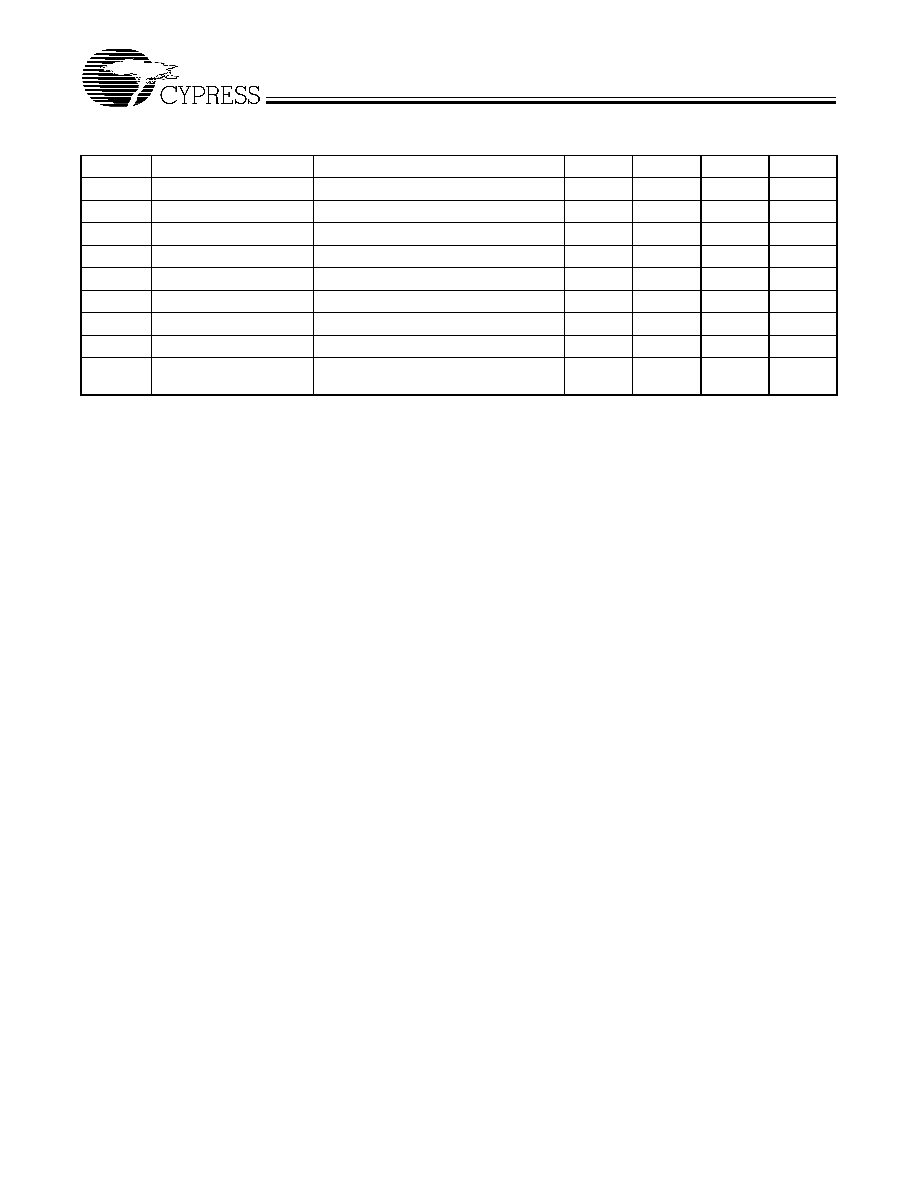
Table 1. Frequency Spread Selection
W42C32-05
FS2
FS1
FS0
REFOUT
(MHz)
CLKOUT
(MHz)
VDD
(V)
0
0
0
22.1148
44.2296 ±
2.5%
5.0
0
0
1
22.1148
44.2296
±1.5%
5.0
0
1
0
14.7456
29.4912 ±
2.5%
5.0
0
1
1
18.432
18.432 ± 2.5%
5.0
1
0
0
14.318
66.66 ≠ 2%
3.3
1
0
1
Reserved
3.3
1
1
0
14.318
100 ≠ 2%
3.3
1
1
1
Reserved
3.3
Pin Configuration
W
42C
32
-05
16
15
14
13
12
11
10
9
1
2
3
4
5
6
7
8
PD#
X1
X2
GND
AGND
FS0
TEST
CLKOUT
REFOUT
FS2
FS1
SSON#
RESET
VDD
AVDD
REFEN#
SOIC
W42C32-05
2
Pin Definitions
[1]
Pin Name
Pin No.
Pin
Type
Pin Description
CLKOUT
8
O
Output Modulated Frequency: Frequency is set using FS0:2 (refer to Table 1).
REFOUT
16
O
Reference Output: A buffered version of the input frequency.
X1
2
I
Crystal Connection or External Reference Frequency Input: This pin has dual func-
tions. It can be used as either an external crystal connection, or as an external reference
frequency input.
X2
3
I
Crystal Connection: If using an external reference, this pin must be left unconnected.
SSON#
13
I
Spread Spectrum Control (active LOW): Pulling this input signal HIGH turns the internal
modulating waveform off. This pin has an internal pull-down resistor.
FS0
6
I
Frequency Selection Bit 0: This pin selects the frequency and spreading characteristics.
Refer to Table 1. This pin has an internal pull-up resistor.
FS1
14
I
Frequency Selection Bit 1: This pin selects the frequency and spreading characteristics.
Refer to Table 1. This pin has an internal pull-up resistor.
FS2
15
I
Frequency Selection Bit 2: This pin selects the frequency and spreading characteristics.
Refer to Table 1 (note the V
DD
specification). This pin has an internal pull-up resistor.
PD#
1
I
Power-down (active LOW): Enabling power-down reduces current consumption and
disables the clock outputs. This pin has an internal pull-up resistor.
REFEN#
9
I
Reference Clock Selection Input: Pulling this signal LOW turns the REFOUT clock
output on. This pin has an internal pull-up resistor.
RESET
12
I
Reset: A reset starts the spread spectrum modulating frequency at the beginning point
of the modulation profile. This pin has an internal pull-down resistor. To reset the spread
spectrum modulating frequency, pull this pin from LOW to HIGH.
VDD
11
P
Power Connection: Connected to either 3.3V or 5.0V power supply. V
DD
and AV
DD
must
be the same voltage level.
AVDD
10
P
Analog Power Connection: Connected to either 3.3V or 5.0V power supply. V
DD
and
AV
DD
must be the same voltage level.
GND
4
G
Ground Connection: Connect to the common system ground plane.
AGND
5
G
Analog Ground Connection: Connect to the common system ground plane.
TEST
7
I
Three-state Input: Pulling this input pin and REFEN# pin HIGH, CLKOUT will be
three-stated. This pin has an internal pull-down resistor.
[2]
Notes:
1.
Pull-up resistors not CMOS level.
2.
Pulling PD# and REFEN# input pins HIGH, REFOUT will be three-stated.

W42C32-05
3
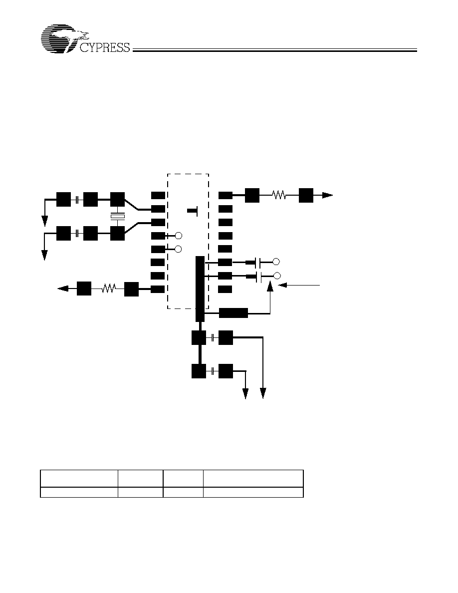
Functional Description
The W42C32-05 uses a phase-locked loop (PLL) to multiply
the frequency of a low-cost, low-frequency crystal up to the
desired clock frequency. The basic circuit topology is shown in
Figure 1. An on-chip crystal driver causes the crystal to oscil-
late at its fundamental. The resulting reference signal is divid-
ed by Q and fed to the phase detector. The VCO output is
divided by P and also fed back to the phase detector. The PLL
will force the frequency of the VCO output signal to change
until the divided output signal and the divided reference signal
match at the phase detector input. The output frequency is
then equal to the ratio of P/Q times the reference frequency.
The unique feature of the Spread Spectrum Frequency Timing
Generator is that a modulating waveform is superimposed at
the input to the VCO. This causes the VCO output to be slowly
swept across a predetermined frequency band.
Because the modulating frequency is typically 1000 times
slower than the fundamental clock, the spread spectrum pro-
cess has little impact on system performance.
Frequency Selection With SSFTG
In Spread Spectrum frequency timing generation, EMI reduc-
tion depends on the shape, modulation percentage, and fre-
quency of the modulating waveform. While the shape and fre-
quency of the modulating waveform in the W42C32 are fixed,
the modulation percentage may be varied.
Using frequency select bits (FS2:0 pins), various spreading
percentages for different input frequency ranges can be cho-
sen. For example, refer to the W42C32-05 in Table 1. If the
logic level on FS2:0 = 000, then an input reference frequency
between 14 and 24 MHz will produce an output frequency at
twice the reference frequency with a spread of ±2.5%.
A larger spreading percentage improves EMI reduction. How-
ever, large spread percentages may either exceed system
maximum frequency ratings or lower the average frequency to
a point where performance is affected. For these reasons,
spreading percentages between ±0.875% and ±2.5% are
most common.
Additional Features of the W42C32-05
A RESET pin is available to aid in applications which have
multiple PLL clock generators. When a reset is issued, the
modulation profile shown in Figure 3 is reset to its starting
point. This feature is necessary for applications in which two
spread spectrum systems must synchronize with each other.
The REFOUT out pin provides a buffered version of the input
clock frequency.
The SSON# pin disables the spread spectrum function when
set to logic HIGH. Otherwise, an internal pull-down resistor
leaves this feature enabled.
The PD# pin reduces power consumption and disables the
clock outputs when set to logic LOW. Otherwise, an internal
pull-up resistor places the W42C32-05 into normal mode.
Figure 1. System Block Diagram (Concept, not actual implementation)
XTAL
Freq.
Phase
Modulating
VCO
Post
CLKOUT
Detector
Charge
Pump
Waveform
Dividers
Divider
Feedback
Divider
PLL
GND
V
DD
X1
X2
Crystal load
capacitors
as needed
Q
P
W42C32-05
4
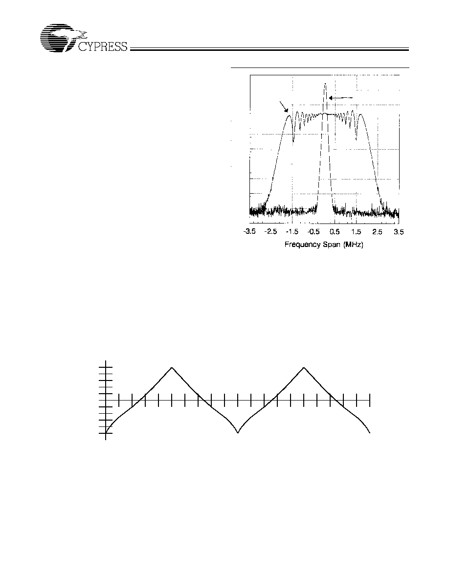
Spread Spectrum Frequency Timing
Generation
The benefits of using Spread Spectrum Frequency Timing
Generation are depicted in Figure 2. An EMI emission profile
of a clock harmonic is shown.
Contrast the typical clock EMI with the Cypress spread spec-
trum clock. Notice the spike in the typical clock. This spike can
make systems fail quasi-peak EMI testing. The FCC and other
regulatory agencies test for peak emissions. With Cypress's
Spread Spectrum Frequency Timing Generator (SSFTG), the
peak energy is much lower (at least 8 dB) because the energy
is spread out across a wider bandwidth.
Modulating Waveform
The shape of the modulating waveform is critical to EMI reduc-
tion. The modulation scheme used to accomplish the maxi-
mum reduction in EMI is shown in Figure 3. The period of the
modulation is shown as a percentage of the period length
along the X axis. The amount that the frequency is varied is
shown along the Y axis, also shown as a percentage of the
total frequency spread.
Cypress frequency selection tables express the modulation
percentage in two ways. The first method displays the spread-
ing frequency band as a percent of the programmed average
output frequency, symmetric about the programmed average
frequency. This method is always shown using the expression
f
Center
±
X
MOD
% in the frequency spread selection table.
The second approach is to specify the maximum operating
frequency and the spreading band as a percentage of this fre-
quency. The output signal is swept from the lower edge of the
band to the maximum frequency. The expression for this ap-
proach is f
MAX
≠
X
MOD
%. Whenever this expression is used,
Cypress has taken care to ensure that f
MAX
will never be ex-
ceeded. This is important in applications where the clock
drives components with tight maximum clock speed specifica-
tions.
SSFTG
Typical Clock
5dB/div
Amp
l
itu
d
e (d
B)
Figure 2. Typical Clock and SSFTG Comparison
100%
60%
20%
80%
40%
0%
≠20%
≠40%
≠60%
≠80%
≠100%
10%
20%
30%
40%
50%
60%
70%
80%
90%
1
00%
10%
20%
30%
40%
50%
60%
70%
80%
90%
1
00%
Time
F
r
e
q
ue
nc
y
S
h
i
f
t
Figure 3. Modulation Waveform Profile
W42C32-05
5
Absolute Maximum Ratings
Stresses greater than those listed in this table may cause per-
manent damage to the device. These represent a stress rating
only. Operation of the device at these or any other conditions
above those specified in the operating sections of this specifi-
cation is not implied. Maximum conditions for extended peri-
ods may affect reliability.
Parameter
Description
Rating
Unit
V
DD
, V
IN
Voltage on any pin with respect to GND
≠0.5 to +7.0
V
T
STG
Storage Temperature
≠65 to +150
∞C
T
A
Operating Temperature
0 to +70
∞C
T
B
Ambient Temperature under Bias
≠55 to +125
∞C
DC Electrical Characteristics:
0∞C < T
A
< 70∞C, V
DD
= 5.0V±10%, 3.3V±5%
Parameter
Description
Test Condition
Min
Typ
Max
Unit
I
DD
Supply Current
V
DD
= 5.0, 100 MHz
35
45
mA
t
OFF
Power Down Time
4
cycles
[3]
t
ON
Power Up Time
First locked clock cycle after
PD# goes HIGH
5
ms
t
EN
Enable/Disable Time
Time required for output to be
enabled/disabled
4
cycles
[3]
V
IL
Input Low Voltage
V
DD
= 5.0V
0.8
V
V
DD
= 3.3V
0.15V
DD
V
V
IH
Input High Voltage
V
DD
= 5.0V
3.0
V
V
DD
= 3.3V
0.7V
DD
V
V
OL
Output Low Voltage
0.4
V
V
OH
Output High Voltage
V
DD
= 5.0V
2.4
V
V
DD
= 3.3V
2.4
V
I
IL
Input Low Current
≠100
µA
I
IH
Input High Current
10
µA
I
OL
Output Low Current
@ 0.4V, V
DD
= 3.3V
2.4
mA
I
OH
Output High Current
@ 2.4V, V
DD
= 3.3V
2.4
mA
C
I
Input Capacitance
All pins except X1, X2
7
pF
C
L
XTAL Load Capacitance
Pins X1, X2
16
pF
R
P
Input Pull-Up Resistor
V
IN
= 0V
300
k
Z
OUT
Clock Output Impedance
Any clock output pin
33
Note:
3.
Cycle refers to input clock cycles supplied by the input crystal or reference.
W42C32-05
6
AC Electrical Characteristics:
T
A
= 0∞C to +70∞C, V
DD
= 5V±10%. 3.3V±5%
Symbol
Parameter
Test Condition
Min
Typ
Max
Unit
f
IN
Input Frequency
12
28
MHz
f
OUT
Output Frequency
18
100
MHz
t
R
Output Rise Time
15-pF load 0.4V≠2.4V
1
2
ns
t
F
Output Fall Time
15-pF load 2.4V≠0.8V
1
2
ns
t
OD
Output Duty Cycle
15-pF load, V
DD
= 5.0V
45
55
%
t
OD
Output Duty Cycle
15-pF load, V
DD
= 3.3V
40
60
%
t
ID
Input Duty Cycle
40
60
%
t
JCYC
Jitter, Cycle-to-Cycle
250
300
ps
Harmonic Reduction
f
in
= 16 MHz, ninth harmonic measured,
reference board, 15-pF load
8
dB
W42C32-05
7
Application Information
Recommended Circuit Configuration
For optimum performance in system applications the power
supply decoupling scheme shown in Figure 4 should be used.
V
DD
decoupling is important to both reduce phase jitter and
EMI radiation. The 0.1-
µ
F decoupling capacitor should be
placed as close to the V
DD
pin as possible, otherwise the in-
creased trace inductance will negate its decoupling capability.
The 10-
µ
F decoupling capacitor shown should be a tantalum
type. For further EMI protection, the V
DD
connection can be
made via a ferrite bead, as shown.
The 16-pF XTAL load capacitors can be used to raise the inte-
grated 12-pF capacitors up to a total load of 20 pF on the
crystal.
Recommended Board Layout
Figure 4 shows a recommended 2-layer board layout.
Document #: 38-00808
Ordering Information
Ordering Code
Freq. Mask
Code
Package
Name
Package Type
W42C32
05
G
16-pin Plastic SOIC (300-mil)
Figure 4. Recommended Board Layout (2-Layer Board)
C
1
=16 pF
C
2
= 16 pF
XTAL1
Typical value is 16 pF.
High frequency supply decoupling
capacitor (0.1-µF recommended).
Common supply low frequency
decoupling capacitor (10-µF tantalum
recommended).
XTAL load capacitors.
C1, C2 =
C3, C5, C6 =
C4 =
Match value to line impedance.
33
=
33
CLKOUT
33
(Modulated Output)
C
4
= 10
µ
F
C
3
= 0.1
µ
F
REFOUT
Ground
Ground
Ferrite Bead
Voltage Supply Input
(3.3V, 5.0V)
1
2
3
4
5
6
7
8
16
15
14
13
12
11
10
9
G
G
G
C5
G
C6
(Via to ground plane)
W42C32-05
© Cypress Semiconductor Corporation, 1999. The information contained herein is subject to change without notice. Cypress Semiconductor Corporation assumes no responsibility for the use
of any circuitry other than circuitry embodied in a Cypress Semiconductor product. Nor does it convey or imply any license under patent or other rights. Cypress Semiconductor does not authorize
its products for use as critical components in life-support systems where a malfunction or failure may reasonably be expected to result in significant injury to the user. The inclusion of Cypress
Semiconductor products in life-support systems application implies that the manufacturer assumes all risk of such use and in doing so indemnifies Cypress Semiconductor against all charges.
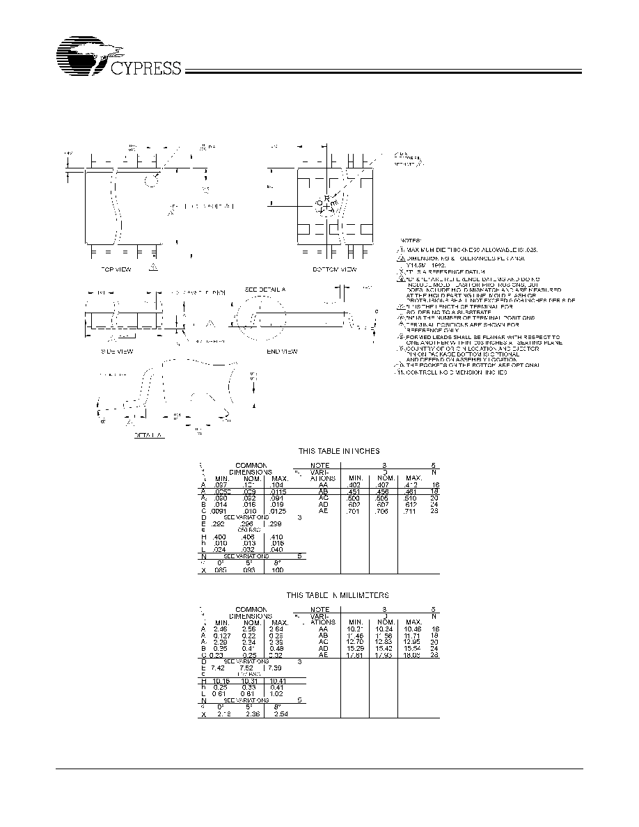
Package Diagram
16-Pin Small Outline Integrated Circuit (SOIC, 300-mil)