 | –≠–ª–µ–∫—Ç—Ä–æ–Ω–Ω—ã–π –∫–æ–º–ø–æ–Ω–µ–Ω—Ç: W48C20 | –°–∫–∞—á–∞—Ç—å:  PDF PDF  ZIP ZIP |
Audio Subsystem Clock Generator
W48C20
Cypress Semiconductor Corporation
∑
3901 North First Street
∑
San Jose
∑
CA 95134
∑
408-943-2600
December 20, 1999, rev. **
Features
∑ Two independent phase-locked loops
∑ Four independent output frequencies
∑ ±250 ps maximum cycle-to-cycle jitter
∑ 3 ns rise/fall time (20%-80% V
DD
).
∑ Options available for a wide range of applications
∑ Supports 3.3V and 5V operation
∑ Low power CMOS design available in:
-- 8-pin SOIC (Small Outline Integrated Circuit)
Overview
The W48C20 is a general-purpose device that features two
phase-locked loops. Through the use of metal masks, the chip
can be tailored to a wide variety of applications.
The W48C20 has four clock outputs, each of which is
maskable to a different frequency. Because the chip offers four
outputs in eight pins, it is suited to applications that require
multiple frequencies and have space constraints.
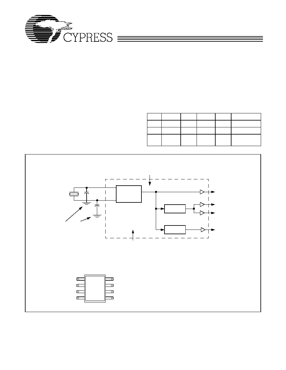
Table 1. Product Selection Guide
Mask
Pin 4
Pin 5
Pin 6
Pin 7
Application
-01A
16.9344 24.576 33.8688 14.318 Audio/Crystal
-08
33.8688 18.432 16.9344
27.00
DVD
-09
40.00
22.50
20.00
25.00
Hard Disk
Drives
Pin Configuration
Functional Block Diagram
XTAL
OSC
OUTPUT
PLL 1
PLL 2
OUTPUT
OUTPUT
OUTPUT
XTAL
X1
X2
Crystal load capacitors
as needed
GND
VCC
X1
VCC
GND
OUTPUT
1
2
3
4
8
7
6
5
X2
OUTPUT
OUTPUT
OUTPUT
W48C20
2
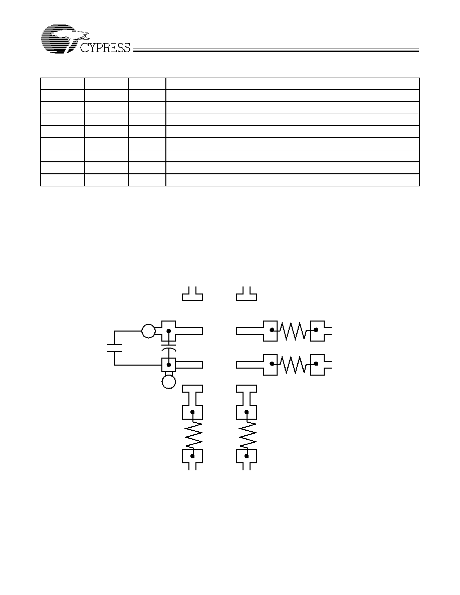
External Components/Crystal Selection
The W48C20 incorporates a crystal oscillator circuit designed
to provide 50% duty cycle over a range of operating conditions,
including the addition of external crystal load capacitors to pins
X1 and X2. A parallel resonant 14.318-MHz, 12-pF load crystal
is recommended. A series-resonant crystal or a parallel reso-
nant crystal specifying a different load can be used, but either
will result in frequencies which are slightly different from the
ideal (up to 0.06%).
The crystal load capacitance can be increased by adding a
capacitor to each of the X1 and X2 pins and ground. This en-
ables the use of a crystal specifying a load greater than 12 pF
without changing the output frequency.
Duty cycle is also maintained when using an external clock
source (connected to X1, X2 left unconnected) as long as the
external clock has good duty cycle. The circuit exhibits about
50% less clock jitter from the 14.318-MHz output when com-
pared to similar devices.
Pin Definitions
Pin Name
Pin No.
Pin Type
Pin Description
X1
1
I
Crystal connection or external clock frequency input (14.318 MHz).
VDD
2
P
Power supply connection.
GND
3
P
Ground connection.
OUTPUT
4
O
16.9344-MHZ clock output for stereo codec.
OUTPUT
5
O
24.576-MHz clock output for stereo codec.
OUTPUT
6
O
33.868-MHz clock output for OPL4.
OUTPUT
7
O
14.318-MHz clock buffered output for OPL3 or PCMCIA controller.
X2
8
I
Crystal connection. Leave this pin unconnected when using an external clock.
14.318 MHz IN
2.2
µ
F
0.1
µ
F
V
G
33
(optional)
16.9 MHz OUT
24.6 MHz OUT
33
(optional)
33
(optional)
33.9 MHz OUT
14.3 MHz OUT
33
(optional)
Pin 1
2
3
4
5
6
7
8
(optional)
Figure 1. Suggested Layout
W48C20
3
Absolute Maximum Ratings
Stresses greater than those listed in this table may cause per-
manent damage to the device. These represent a stress rating
only. Operation of the device at these or any other conditions
above those specified in the operating sections of this specifi-
cation is not implied. Maximum conditions for extended peri-
ods may affect reliability
Electrical Characteristics at 5.0V
Document #: 38-00879
Parameter
Description
Rating
Unit
V
CC
, V
IN
Voltage on any Pin with Respect to GND
≠0.5 to +7.0
V
T
STG
Storage Temperature
≠65 to +150
∞C
T
A
Operating Temperature
0 to +70
∞C
T
B
Ambient Temperature under Bias
≠55 to +125
∞C
T
SOLD
Soldering Temperature, Max. 20 seconds
260
∞C
DC Electrical Characteristics:
T
A
= 0∞C to +70∞C; V
CC
= 5V ± 10%
Parameter
Description
Conditions
Min
Typ
Max
Unit
V
DD
Operating Voltage
4.5
5.5
V
V
IH
Input High Voltage
3.5
2.5
V
V
IL
Input Low Voltage
2.5
1.5
V
V
OH
Output High Voltage
I
OH
= 25 mA
2.4
V
V
OL
Output Low Voltage
I
OL
= 25 mA
0.4
V
I
DD
Operating Supply Current
No Load
18
mA
Input Capacitance
[1]
7
pF
Actual Mean Frequency versus Target
±0.2
%
AC Characteristics:
T
A
= 0∞C to +70∞C; V
CC
= 5V ± 10%
Parameter
Test Condition/Comments
Min
Typ
Max
Unit
Input Clock Frequency
14.31818
MHz
Input Clock Duty Cycle, 14.318 MHz
Time above 2.5V
20
80
%
Output Clock Rise Time
0.8V to 2.0V
1.5
ns
Output Clock Fall Time
2.0V to 0.8V
1.5
ns
Output Clock Duty Cycle, 24.576 MHz
Time above 1.5V
40
45
60
%
Output Clock Duty Cycle, 16.9344 MHz
Time above 1.5V
45
50
55
%
Output Clock Duty Cycle, 33.868 MHz
Time above 1.5V
45
50
55
%
Output Clock Duty Cycle, 14.318 MHz
[2]
Time above 1.5V
45
50
55
%
Absolute Clock Period Jitter, except 14.3
Pins 4, 5, 6 only
≠400
200
400
ps
One Sigma Clock Period Jitter, except 14.3 Pins 4, 5, 6 only
60
ps
Notes:
1.
If crystal is used as input Crystal Load Capacitance (C
L
) = 12 pF.
2.
If a clock is used as input, the duty cycle of the 14.318-MHz output will be the same as the input clock.
Ordering Information
Ordering Code
Freq. Mask
Code
Package
Name
Package Type
W48C20
01A
08
09
G
8-pin SOIC (150-mil)

W48C20
© Cypress Semiconductor Corporation, 1999. The information contained herein is subject to change without notice. Cypress Semiconductor Corporation assumes no responsibility for the use
of any circuitry other than circuitry embodied in a Cypress Semiconductor product. Nor does it convey or imply any license under patent or other rights. Cypress Semiconductor does not authorize
its products for use as critical components in life-support systems where a malfunction or failure may reasonably be expected to result in significant injury to the user. The inclusion of Cypress
Semiconductor products in life-support systems application implies that the manufacturer assumes all risk of such use and in doing so indemnifies Cypress Semiconductor against all charges.
Package Diagram
8-Pin Small Outline Integrated Circuit, Narrow (SOIC, 0.150 inch)