 | –≠–ª–µ–∫—Ç—Ä–æ–Ω–Ω—ã–π –∫–æ–º–ø–æ–Ω–µ–Ω—Ç: W48S87 | –°–∫–∞—á–∞—Ç—å:  PDF PDF  ZIP ZIP |
PRELIMINARY
Spread Spectrum 3 DIMM Desktop Clock
W48S87-04
Cypress Semiconductor Corporation
∑
3901 North First Street
∑
San Jose
∑
CA 95134
∑
408-943-2600
October 19, 1999, rev. **
Features
∑ Outputs
-- 4 CPU Clock (2.5V or 3.3V, 50 to 83.3 MHz)
-- 7 PCI (3.3V)
-- 1 48-MHz for USB (3.3V)
-- 1 24-MHz for Super I/O (3.3V)
-- 2 REF (3.3V)
-- 1 IOAPIC (2.5V or 3.3V)
-- 12 SDRAM
∑ Serial data interface provides additional frequency
selection, individual clock output disable, and other
functions
∑ Smooth transition supports dynamic frequency
assignment
∑ Frequency selection not affected during power
down/up cycle
∑ Supports a variety of power-saving options
∑ 3.3V operation
∑ Available in 48-pin SSOP (300 mils)
Key Specifications
±0.5% Spread Spectrum Modulation: ......................... ±0.5%
Jitter (Cycle-to-Cycle): .................................................250 ps
Duty Cycle: ................................................................ 45-55%
CPU-PCI Skew: ........................................................ 1 to 4 ns
PCI-PCI or CPU-CPU Skew: .......................................250 ps
Notes:
1.
Additional frequency selections provided by serial data interface; refer to Table 5 on page 10.
2.
Signal names in parenthesis denotes function is selectable through mode pin register strapping.
Table 1. Pin Selectable Frequency
[1]
Input Address
CPU, SDRAM
Clocks (MHz)
PCI Clocks
(MHz)
FS2
FS1
FS0
0
0
0
50.0
25.0
0
0
1
75.0
32.0
0
1
0
83.3
41.65
0
1
1
68.5
34.25
1
0
0
55.0
27.5
1
0
1
75.0
37.5
1
1
0
60.0
30.0
1
1
1
66.8
33.4
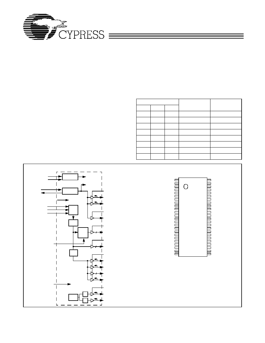
Block Diagram
Pin Configuration
[2]
VDD1
IOAPIC
VDD3
SDRAM0:11
PCI_F/FS1
PCI0/FS2
XTAL OSC
PLL Ref
PLL1
X2
X1
REF1(CPU_STOP#)
Stop
Clock
Cntrl
PCI1:4
PWR_DWN#
Power Down
Control
PCI5(PWR_DWN#)
48MHZ/FS0
24MHZ/MODE
PLL2
Serial Port
SCLOCK
SDATA
Device
CPU_STOP#
Control
CPU3.3#_2.5
CPU Clock
Mode Control
˜4
˜2
I/O
I/O
VDD1
MODE
4
I/O
I/O
VDD2
12
CPU0:3
4
VDDL2
˜2
VDDL1
MODE
I/O
REF0/CPU3.3#_2.5
Freq
Select
FS0
FS1
FS2
Freq
VDD1
REF0/CPU3.3#_2.5
GND
X1
X2
VDD2
PCI_F/FS1
PCI0/FS2
GND
PCI1
PCI2
PCI3
PCI4
VDD2
PCI5(PWR_DWN#)
GND
SDRAM11
SDRAM10
VDD3
SDRAM9
SDRAM8
GND
SDATA
SCLOCK
W
4
8S
87
-04
VDDL1
IOAPIC
REF1(CPU_STOP#)
GND
CPU0
CPU1
VDDL2
CPU2
CPU3
GND
SDRAM0
SDRAM1
VDD3
SDRAM2
SDRAM3
GND
SDRAM4
SDRAM5
VDD3
SDRAM6
SDRAM7
GND
48MHZ/FS0
24MHZ/MODE
48
47
46
45
44
43
42
41
40
39
38
37
36
35
34
33
32
31
30
29
28
27
26
25
1
2
3
4
5
6
7
8
9
10
11
12
13
14
15
16
17
18
19
20
21
22
23
24
W48S87-04
PRELIMINARY
2
Pin Definitions
Pin Name
Pin
No.
Pin
Type
Pin Description
CPU0:3
44, 43, 41,
40
O
CPU Clock Outputs 0 through 3: These four CPU clock outputs are controlled
by the CPU_STOP# control pin. Output voltage swing is controlled by voltage
applied to VDDL2 and output characteristics are adjusted by input
CPU3.3#_2.5.
PCI_F/FS1
7
I/O
Fixed PCI Clock Output and Frequency Selection Bit 1: As an output, this
pin works in conjunction with PCI0:5. Output voltage swing is controlled by
voltage applied to VDD2.
When an input, this pin functions as part of the frequency selection address.
The value of FS0:2 determines the power-up default frequency of device output
clocks as per the Table 1, "Pin Selectable Frequency" on page 1.
PCI0/FS2
8
I/O
PCI Bus Clock Output 0 and Frequency Selection Bit 2: As an output, this
pin works in conjunction with PCI1:5 and PCI_F. Output voltage swing is con-
trolled by voltage applied to VDD2.
When an input, this pin functions as part of the frequency selection address.
The value of FS0:2 determines the power-up default frequency of device output
clocks as per the Table 1, "Pin Selectable Frequency" on page 1.
PCI1:4
10, 11, 12,
13
O
PCI Bus Clock Outputs 1 through 4: Output voltage swing is controlled by
voltage applied to VDD2.
PCI5(PWR_DWN#)
15
I/O
PCI Bus Clock Output 5 or Power-Down Control: As an output, this pin works
in conjunction with PCI0:4 and PCI_F. Output voltage swing is controlled by
voltage applied to VDD2.
If programmed as an input (refer to MODE pin description), this pin is used for
power-down control. When LOW, the device goes into a low-power standby
condition. All outputs are actively held LOW while in power-down. CPU,
SDRAM, and PCI clock outputs are stopped LOW after completing a full clock
cycle (2≠4 CPU clock cycle latency). When brought HIGH, CPU, SDRAM, and
PCI outputs start with a full clock cycle at full operating frequency (3 ms max-
imum latency).
SDRAM0:11
38, 37, 35,
34, 32, 31,
29, 28, 21,
20, 18, 17
O
SDRAM Clock Outputs 0 through 11: These twelve SDRAM clock outputs
run synchronous to the CPU clock outputs. Output voltage swing is controlled
by voltage applied to VDD3.
IOAPIC
47
O
I/O APIC Clock Output: Provides 14.318-MHz fixed frequency. The output
voltage swing is controlled by VDDL1.
48MHZ/FS0
26
I/O
48-MHz Output and Frequency Selection Bit 0: Fixed clock output that de-
faults to 48 MHz following device power-up. Output voltage swing is controlled
by voltage applied to VDD1.
When an input, this pin functions as part of the frequency selection address.
The value of FS0:2 determines the power-up default frequency of device output
clocks as per the Table 1, "Pin Selectable Frequency" on page 1.
24MHZ/MODE
25
I/O
24-MHz Output and Mode Control Input: Fixed clock output that defaults to
24 MHz following device power-up. Output voltage swing is controlled by volt-
age applied to VDD1.
When an input, this pin is used for pin programming selection. It determines
the functions for pins 15 and 46:
MODE
Pin 15
Pin 46
0
PWR_DWN# (input)
CPU_STOP# (input)
1
PCI5 (output)
REF1 (output)
W48S87-04
PRELIMINARY
3
REF0/CPU3.3#_2.5
2
I/O
Fixed 14.318-MHz Output 0 and CPU Output Voltage Swing Selection
Input: As an output, this pin is used for various system applications. Output
voltage swing is controlled by voltage applied to VDD1. REF0 is stronger than
REF1 and should be used for driving ISA slots.
When an input, this pin selects the CPU clock output buffer characteristics that
are optimized for either 3.3V or 2.5V operation.
CPU3.3#_2.5
VDDQ2 Voltage (CPU0:3 Swing)
0
3.3V
1
2.5V
This input adjusts CPU clock output impedance so that a nominal 20
output
impedance is maintained. This eliminates or reduces the need to adjust exter-
nal clock tuning components when changing VDDL2 voltage. CPU clock phase
is also adjusted so that both CPU and SDRAM and CPU-to-PCI clock skew is
maintained over the two VDDL2 voltage options. This input does not adjust
IOAPIC clock output characteristics.
REF1(CPU_Stop#)
46
I/O
Fixed 14.318-MHz Output 0 or CPU Clock Output Stop Control: Used for
various system applications. Output voltage swing is controlled by voltage ap-
plied to VDD1. REF0 is stronger than REF1 and should be used for driving ISA
slots.
If programmed as an input (refer to MODE pin description), this pin is used for
stopping the CPU clock outputs. When brought LOW, clock outputs CPU0:3
are stopped LOW after completing a full clock cycle (2≠3 CPU clock latency).
When brought HIGH, clock outputs CPU0:3 are starting beginning with a full
clock cycle (2≠3 CPU clock latency).
X1
4
I
Crystal Connection or External Reference Frequency Input: This pin has
dual functions. It can be used as an external 14.318-MHz crystal connection
or as an external reference frequency input.
X2
5
I
Crystal Connection: An input connection for an external 14.318-MHz crystal.
If using an external reference, this pin must be left unconnected.
SDATA
23
I
Serial Data Input: Data input for Serial Data Interface. Refer to Serial Data
Interface section that follows.
SCLOCK
24
I
Serial Clock Input: Clock input for Serial Data Interface. Refer to Serial Data
Interface section that follows.
VDD1
1
P
Power Connection: Power supply for crystal oscillator and REF0:1 output
buffers. Connected to 3.3V supply.
VDD2
6,14
P
Power Connection: Power supply for PCI clock output buffers. Connected to
3.3V supply.
VDDL1
48
P
Power Connection: Power supply for IOAPIC output buffer. Connected to 2.5V
or 3.3V supply.
VDDL2
42
P
Power Connection: Power supply for CPU clock output buffers. Connected to
2.5V or 3.3V supply.
VDD3
19, 30, 36
P
Power Connection: Power supply for SDRAM clock output buffers. Connected
to 3.3V supply.
GND
3, 9, 16, 22,
27, 33, 39,
45
G
Ground Connection: Connect all ground pins to the common system ground
plane.
Pin Definitions
(continued)
Pin Name
Pin
No.
Pin
Type
Pin Description

W48S87-04
PRELIMINARY
4
Overview
The W48S87-04, a motherboard clock synthesizer, can pro-
vide either a 2.5V or 3.3V CPU clock swing, making it suitable
for a variety of CPU options. Twelve SDRAM clocks are pro-
vided in phase with the CPU clock outputs. This provides clock
support for up to three SDRAM DlMMs. Fixed output frequency
clocks are provided for other system functions.
Functional Description
I/O Pin Operation
Pins 2, 7, 8, 25, and 26 are dual-purpose l/O pins. Upon power-
up these pins act as logic inputs, allowing the determination of
assigned device functions. A short time after power-up, the
logic state of these pins is latched and the pins then become
clock outputs. This feature reduces device pin count by com-
bining clock outputs with input select pins.
An external 10-k
"strapping" resistor is connected between
each l/O pin and ground or V
DD3
. Connection to ground sets a
latch to "0", connection to V
DD3
sets a latch to "1". Figure 1 and
Figure 2 show two suggested methods for strapping resistor
connection.
Upon W48S87-04 power-up, the first 2 ms of operation is used
for input logic selection. During this period, these dual-purpose
I/O pins are three-stated, allowing the output strapping resistor
on each l/O pin to pull the pin and its associated capacitive
clock load to either a logic HIGH or LOW state. At the end of
the 2-ms period, the established logic 0 or 1 condition of each
l/O is pin is then latched. Next the output buffers are enabled,
which converts the l/O pins into operating clock outputs. The
2-ms timer is started when V
DD
reaches 2.0V. The input bits
can only be reset by turning V
DD
off and then back on again.
It should be noted that the strapping resistors have no signifi-
cant effect on clock output signal integrity. The drive imped-
ance of both clock outputs is <40
(nominal) which is minimal-
ly affected by the 10-k
strap to ground or V
DD
. As with the
series termination resistor, the output strapping resistor should
be placed as close to the l/O pin as possible in order to keep
the interconnecting trace short. The trace from the resistor to
ground or VDD should be kept less than two inches in length
to prevent system noise coupling during input logic sampling.
When the clock outputs are enabled following the 2-ms input
period, target (normal) output frequency is delivered assuming
that V
DD
has stabilized. If V
DD
has not yet reached full value,
output frequency initially may be below target but will increase
to target once V
DD
voltage has stabilized. In either case, a
short output clock cycle may be produced from the CPU clock
outputs when the outputs are enabled.
Power-on
Reset
Timer
Output Three-state
Data
Latch
Hold
Q
D
W48S87-04
V
DD
Clock Load
22
10 k
Output
Buffer
(Load Option 1)
10 k
(Load Option 0)
Output
Low
Output Strapping Resistor
Series Termination Resistor
Figure 1. Input Logic Selection Through Resistor Load Option
Power-on
Reset
Timer
Output Three-state
Data
Latch
Hold
Q
D
W48S87-04
V
DD
Clock Load
R
10 k
Output
Buffer
Output
Low
Output Strapping Resistor
Series Termination Resistor
Jumper Options
Figure 2. Input Logic Selection Through Jumper Option
Resistor Value R
39
33
Output
IOAPIC, SDRAM
All other clock outputs

W48S87-04
PRELIMINARY
5
CPU/PCI Frequency Selection
CPU frequency is selected with I/O pins 26, 7, and 8
(48MHz/FS0, PCI_F/FS1, and PCI0/FS2, respectively). Refer
to Table 1 for CPU/PCI frequency programming information.
Additional frequency selections are available through the seri-
al data interface. Refer to Table 5 on page 10.
Output Buffer Configuration
Clock Outputs
All clock outputs are designed to drive serial terminated clock
lines. The W48S87-04 outputs are CMOS-type, which provide
rail-to-rail output swing. To accommodate the limited voltage
swing required by some processors, the output buffers of
CPU0:3 use a special VDDL2 power supply pin that can be
tied to 2.5V nominal.
Crystal Oscillator
The W48S87-04 requires one input reference clock to synthe-
size all output frequencies. The reference clock can be either
an externally generated clock signal or the clock generated by
the internal crystal oscillator. When using an external clock
signal, pin X1 is used as the clock input and pin X2 is left open.
The input threshold voltage of pin X1 is V
DD
/2.
The internal crystal oscillator is used in conjunction with a
quartz crystal connected to device pins X1 and X2. This forms
a parallel resonant crystal oscillator circuit. The W48S87-04
incorporates the necessary feedback resistor and crystal load
capacitors. Including typical stray circuit capacitance, the total
load presented to the crystal is approximately 20 pF. For opti-
mum frequency accuracy without the addition of external ca-
pacitors, a parallel-resonant mode crystal specifying a load of
20 pF should be used. This will typically yield reference fre-
quency accuracies within ±100 ppm.
Dual Supply Voltage Operation
The W48S87-04 is designed for dual power supply operation.
Supply pins VDD1, VDD2, and VDD3 are connected to a 3.3V
supply and supply power to the internal core circuit and to the
clock output buffers, except for outputs CPU0:3 and IOAPIC.
Supply pins VDDL1 and VDDL2 may be connected to either a
2.5V or 3.3V supply.