CYStech Electronics Corp.
Spec. No. : C599N3
Issued Date : 2005.12.30
Revised Date :
Page No. : 1/4
BTA1542N3
CYStek Product Specification
PNP Epitaxial Planar Transistor
BTA1542N3
Description
∑
Large current capability
∑
Low collector-to-emitter saturation voltage.
∑
High speed switching.
∑
Ultra-small package facilitates miniaturization in end products.
∑
High allowable power dissipation.
∑
Pb-free package
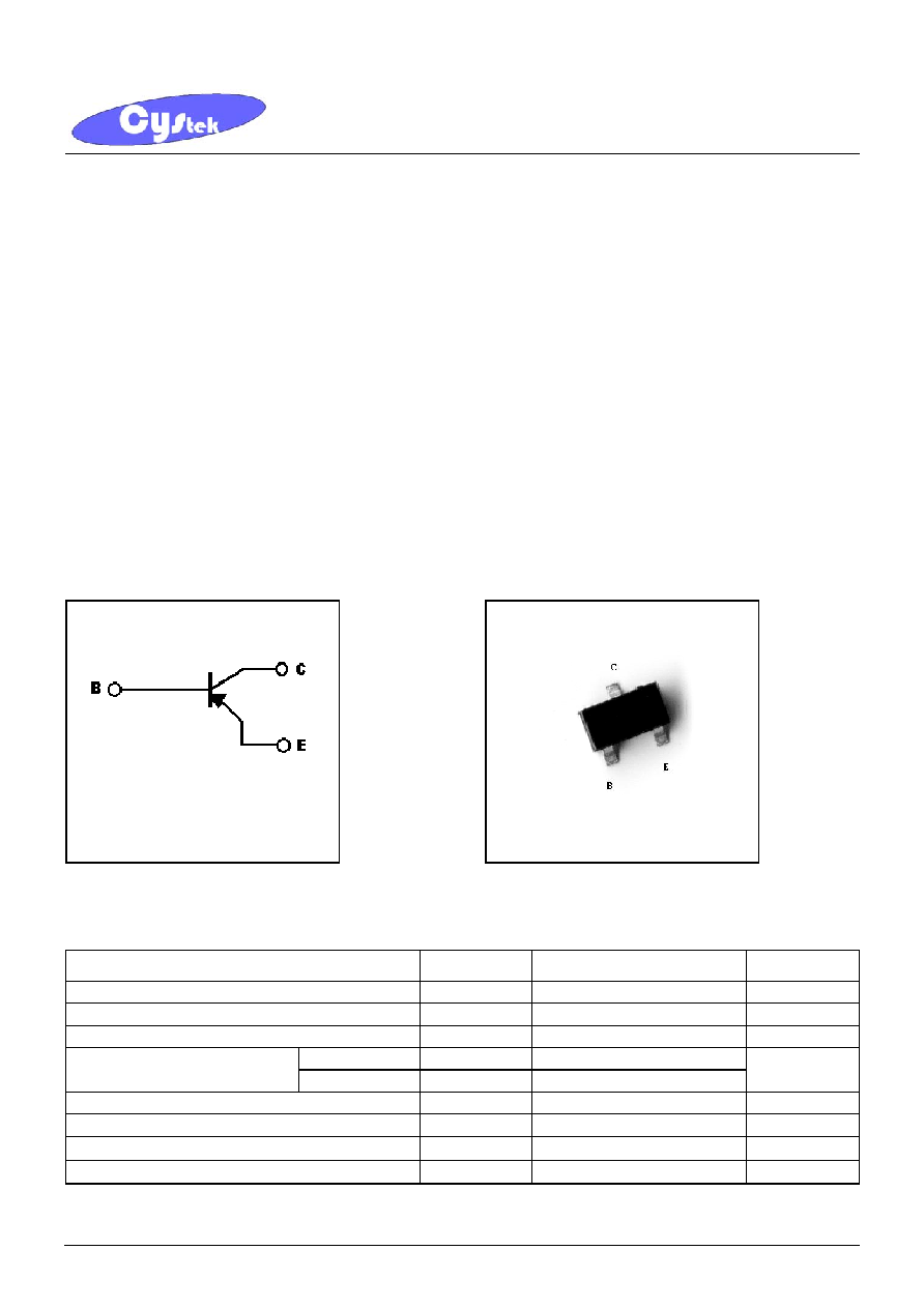
Symbol Outline
Absolute Maximum Ratings
(Ta=25
∞
C)
Parameter Symbol
Limits
Unit
Collector-Base Voltage
V
CBO
-30 V
Collector-Emitter Voltage
V
CEO
-20 V
Emitter-Base Voltage
V
EBO
-5 V
DC I
C
-3
Collector Current
Pulse I
CP
-5
A
Base Current
I
B
-600 mA
Power Dissipation
Pd
0.9
(Note)
W
Junction Temperature
Tj
150
∞
C
Storage Temperature
Tstg
-55~+150
∞
C
Note : When device mounted on a ceramic board (600mm≤◊0.8mm)
BTA1542N3
SOT-23
BBase
CCollector
EEmitter
CYStech Electronics Corp.
Spec. No. : C599N3
Issued Date : 2005.12.30
Revised Date :
Page No. : 2/4
BTA1542N3
CYStek Product Specification
Characteristics
(Ta=25
∞
C)
Symbol Min.
Typ.
Max.
Unit
Test
Conditions
BV
CBO
-30 -
- V I
C
=-10µA
BV
CEO
-20 -
- V
I
C
=-1mA
BV
EBO
-5 - - V
I
E
=-10µA
I
CBO
- - -100
nA
V
CB
=-30V
I
EBO
- -
-100
nA
V
EB
=-4V
V
CE(sat)
1 -
- -230 mV
I
C
=-1.5A, I
B
=-30mA
*V
CE(sat)
2 -
- -155 mV
I
C
=-1.5mA, I
B
=-75mA
*V
BE(sat)
- - -1.2 V
I
C
=-1.5A, I
B
=-30mA
h
FE
1 200 - 560 -
V
CE
=-2V, I
C
=-500mA
f
T
-
380
-
MHz
V
CE
=-10V, I
C
=-500mA
Cob - 25 - pF
V
CB
=-10V, I
E
=0A,f=1MHz
ton - 50 - ns
tstg -
270
- ns
tf -
25
-
ns
V
CC
=-12V, R
L
=24,
I
C
=-20I
B
1=20I
B
2=-500mA
*Pulse Test: Pulse Width
380µs, Duty Cycle
2%
Ordering Information
Device Package
Shipping
Marking
BTA1542N3
SOT-23
(Pb-free)
3000 pcs / Tape & Reel
SH
CYStech Electronics Corp.
Spec. No. : C599N3
Issued Date : 2005.12.30
Revised Date :
Page No. : 3/4
BTA1542N3
CYStek Product Specification
Reel Dimension
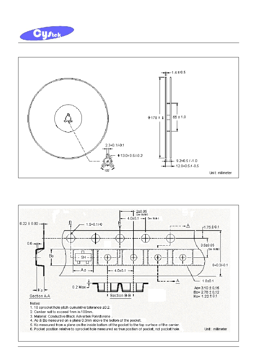
Carrier Tape Dimension
CYStech Electronics Corp.
Spec. No. : C599N3
Issued Date : 2005.12.30
Revised Date :
Page No. : 4/4
BTA1542N3
CYStek Product Specification
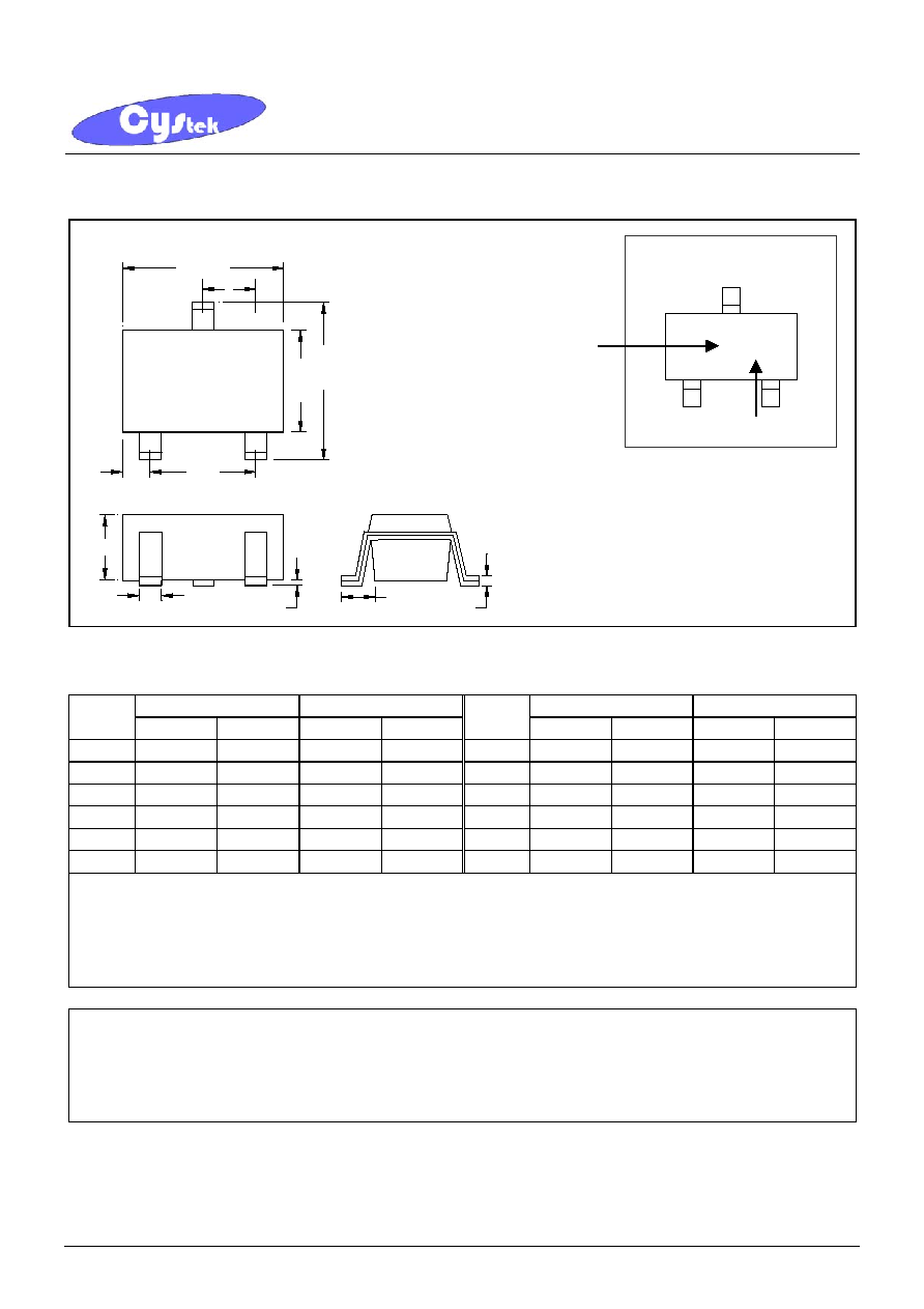
SOT-23 Dimension
*: Typical
Inches Millimeters
Inches Millimeters
DIM
Min. Max. Min. Max.
DIM
Min. Max. Min. Max.
A 0.1102
0.1204 2.80 3.04 J 0.0034
0.0070 0.085 0.177
B 0.0472
0.0630 1.20 1.60 K 0.0128
0.0266 0.32 0.67
C 0.0335
0.0512 0.89 1.30 L 0.0335
0.0453 0.85 1.15
D 0.0118
0.0197 0.30 0.50 S 0.0830
0.1083 2.10 2.75
G 0.0669
0.0910 1.70 2.30 V 0.0098
0.0256 0.25 0.65
H
0.0005
0.0040
0.013
0.10
Notes:
1.Controlling dimension: millimeters.
2.Maximum lead thickness includes lead finish thickness, and minimum lead thickness is the minimum thickness of base material.
3.If there is any question with packing specification or packing method, please contact your local CYStek sales office.
Material:
∑
Lead: 42 Alloy ; solder plating
∑
Mold Compound: Epoxy resin family, flammability solid burning class: UL94V-0
Important Notice:
∑
All rights are reserved. Reproduction in whole or in part is prohibited without the prior written approval of CYStek.
∑
CYStek reserves the right to make changes to its products without notice.
∑
CYStek semiconductor products are not warranted to be suitable for use in Life-Support Applications, or systems.
∑
CYStek assumes no liability for any consequence of customer product design, infringement of patents, or application assistance.
H
J
K
D
A
L
G
V
C
B
3
2
1
S
Style: Pin 1.Base 2.Emitter 3.Collector
Marking:
TE
3-Lead SOT-23 Plastic
Surface Mounted Package
CYStek Package Code: N3
SH xx
Date code
Type name