 | –≠–ª–µ–∫—Ç—Ä–æ–Ω–Ω—ã–π –∫–æ–º–ø–æ–Ω–µ–Ω—Ç: BTB772SA3 | –°–∫–∞—á–∞—Ç—å:  PDF PDF  ZIP ZIP |
CYStech Electronics Corp.
Spec. No. : C817A3-H
Issued Date : 2003.05.31
Revised D
ate:
2004.07.02
Page:1/4
BTB772SA3
CYStek Product Specification
Low Vcesat PNP Epitaxial Planar Transistor
BTB772SA3
Features
∑
Low V
CE
(sat),typically -0.3 V at I
C
/ I
B
= -2A / -0.2A
∑
Excellent current gain characteristics
∑
Complementary to BTD882SA3
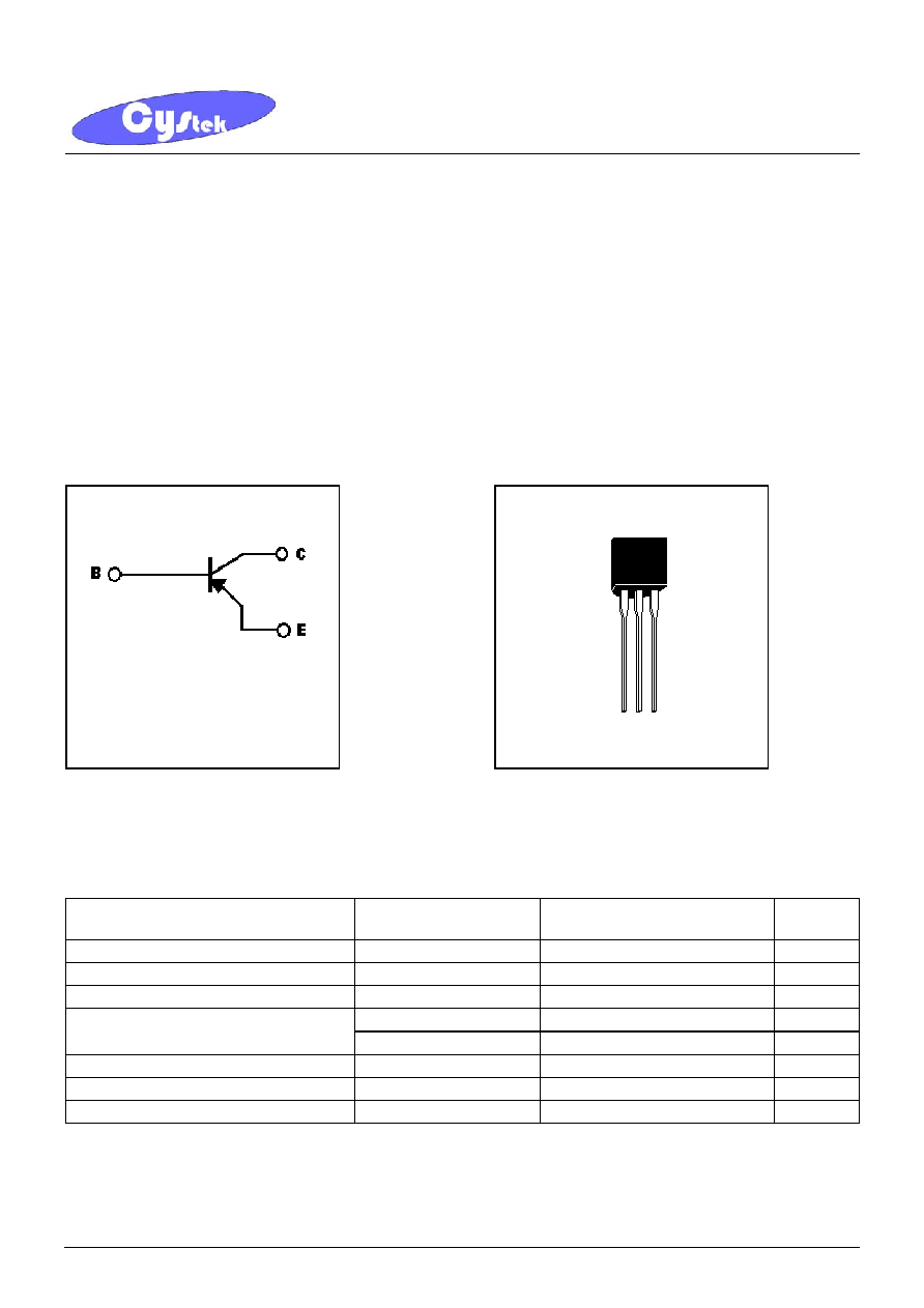
Symbol Outline
Absolute Maximum Ratings
(Ta=25
∞
C)
Parameter Symbol
Limit
Unit
Collector-Base Voltage
V
CBO
-50
V
Collector-Emitter Voltage
V
CEO
-50
V
Emitter-Base Voltage
V
EBO
-5
V
I
C
(DC) -3
A
Collector Current
I
C
(pulse)
-7
(Note)
A
Power Dissipation
Pd
750
mW
Junction Temperature
Tj
150
∞
C
Storage Temperature
Tstg
-55~+150
∞
C
Note : Single Pulse Pw350
µ
s, Duty2%.
BTB772SA3
TO-92
BBase
CCollector
EEmitter
E C B
CYStech Electronics Corp.
Spec. No. : C817A3-H
Issued Date : 2003.05.31
Revised D
ate:
2004.07.02
Page:2/4
BTB772SA3
CYStek Product Specification
Characteristics
(Ta=25
∞
C)
Symbol Min. Typ. Max. Unit
Test
Conditions
BV
CBO
-50 - - V
I
C
=-50µA, I
E
=0
BV
CEO
-50 - - V
I
C
=-1mA, I
B
=0
BV
EBO
-5 - - V
I
E
=-50µA, I
C
=0
I
CBO
- - -1
µA
V
CB
=-30V, I
E
=0
I
EBO
- - -1
µA
V
EB
=-3V, I
C
=0
*V
CE(sat)
- -0.3
-0.5 V
I
C
=-2A, I
B
=-0.2A
*V
BE(sat)
- -1 -2 V
I
C
=-2A, I
B
=-0.2A
*h
FE
1 52 - - -
V
CE
=-2V, I
C
=-20mA
*h
FE
2 100 - 500 -
V
CE
=-2V, I
C
=-1A
f
T
-
80
-
MHz
V
CE
=-5V, I
C
=-0.1A, f=100MHz
Cob - 55
-
pF
V
CB
=-10V, f=1MHz
*Pulse Test : Pulse Width
380
µ
s, Duty Cycle
2%
Classification Of h
FE
2
Rank Q
P
E
Range 100~200 160~320 250~500
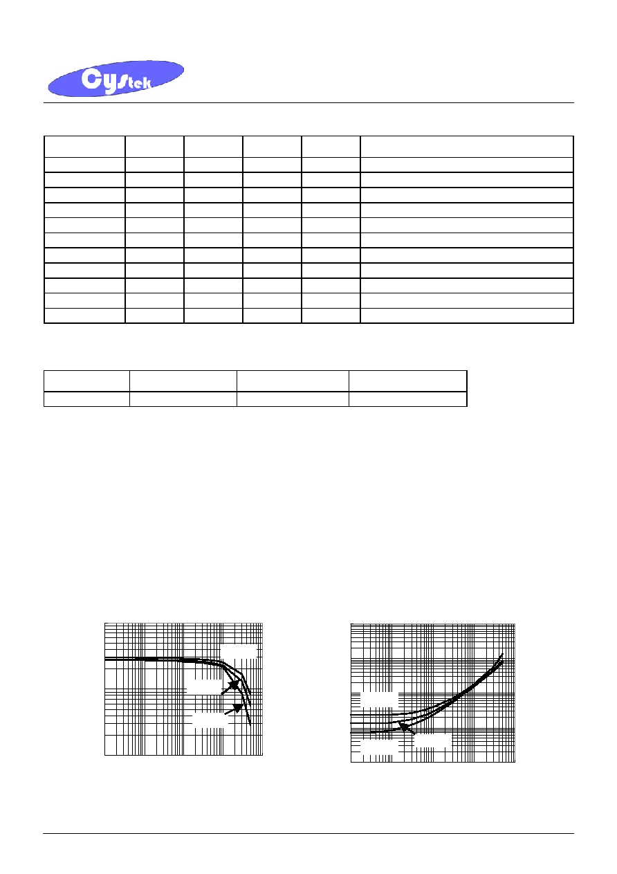
Characteristic Curves
Current gain vs Collector current
10
100
1000
1
10
100
1000
10000
Collector current---IC(mA)
Current gain---H
FE
VCE=5V
VCE=2V
VCE=1V
C-E saturation voltage vs Collector current
1
10
100
1000
10000
1
10
100
1000
10000
Collector current---IC(mA)
C-E saturation voltage---VCE(SAT)(m
V)
IC=40IB
IC=20IB
IC=10IB
CYStech Electronics Corp.
Spec. No. : C817A3-H
Issued Date : 2003.05.31
Revised D
ate:
2004.07.02
Page:3/4
BTB772SA3
CYStek Product Specification
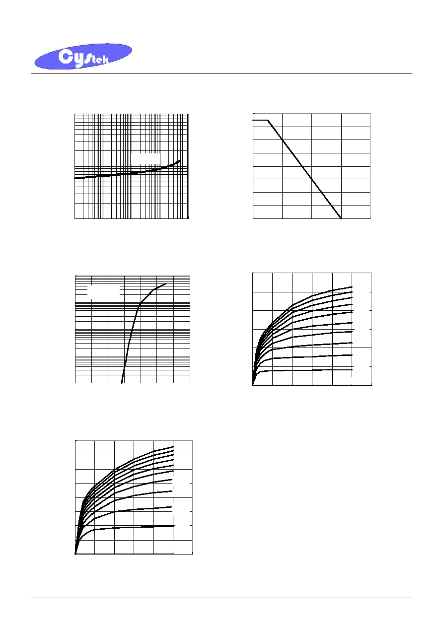
B-E saturation voltage vs Collector current
100
1000
10000
1
10
100
1000
10000
Collector current---IC(mA)
B-E saturation---VBE(SAT)(mV)
IC=10IB
Power Derating Curve
0
100
200
300
400
500
600
700
800
0
50
100
150
200
Ambient Temperature --- Ta( )
Power Dissipation---PD(mW
)
Grounded Emitter Propagation Characteristics
1
10
100
1000
10000
0
200
400
600
800 1000 1200 1400
Base To Emitter Voltage---VBE(V)
Collector Current---IC(m
A)
VCE = 2V
Grounded Emitter Output Characteristics
0
500
1000
1500
2000
2500
3000
0
1
2
3
4
5
6
Collector To Emitter Voltage---VCE(V)
Collector Current---IC(m
A)
IB=0mA
2mA
4mA
6mA
8mA
10mA
12mA
14mA
16mA
18mA
20mA
Grounded Emitter Output Characteristics
0
500
1000
1500
2000
2500
3000
3500
4000
0
1
2
3
4
5
6
Collector To Emitter Voltage---VCE(V)
Collector Current---IC(m
A)
IB=0mA
5mA
10mA
15mA
20mA
25mA
30mA
35mA
40mA
45mA
50mA
CYStech Electronics Corp.
Spec. No. : C817A3-H
Issued Date : 2003.05.31
Revised D
ate:
2004.07.02
Page:4/4
BTB772SA3
CYStek Product Specification
TO-92 Dimension
*: Typical
Inches Millimeters
Inches Millimeters
DIM
Min. Max. Min. Max.
DIM
Min. Max. Min. Max.
A 0.1704
0.1902 4.33 4.83 G 0.0142 0.0220 0.36 0.56
B 0.1704
0.1902 4.33 4.83 H
-
*
0.1000 -
*
2.54
C 0.5000 - 12.70 -
I
-
*
0.0500 -
*
1.27
D 0.0142
0.0220 0.36 0.56
1
-
*
5
∞
-
*
5
∞
E -
*
0.0500 -
*
1.27
2
-
*
2
∞
-
*
2
∞
F 0.1323
0.1480 3.36 3.76
3
-
*
2
∞
-
*
2
∞
Notes:
1.Controlling dimension: millimeters.
2.Maximum lead thickness includes lead finish thickness, and minimum lead thickness is the minimum thickness of base material.
3.If there is any question with packing specification or packing method, please contact your local CYStek sales office.
Material:
∑
Lead: 42 Alloy ; solder plating
∑
Mold Compound: Epoxy resin family, flammability solid burning class: UL94V-0
Important Notice:
∑
All rights are reserved. Reproduction in whole or in part is prohibited without the prior written approval of CYStek.
∑
CYStek reserves the right to make changes to its products without notice.
∑
CYStek semiconductor products are not warranted to be suitable for use in Life-Support Applications, or systems.
∑
CYStek assumes no liability for any consequence of customer product design, infringement of patents, or application assistance.
B772S
Marking:
3
1
A
D
B
C
I
1
E
F
2
3
G
H
2
Style: Pin 1.Emitter 2.Collector 3.Base
3-Lead TO-92 Plastic Package
CYStek Package Code: A3