CYStech Electronics Corp.
Spec. No. : C213S3
Issued Date : 2003.04.25
Revised Date :
Page No. : 1/3
BTC5179S3
CYStek Product Specification
High Frequency NPN Epitaxial Planar Transistor
BTC5179S3
Description
The BTC5179S3 is a NPN Epitaxial Silicon Transistor designed for low noise microwave amplification
application.
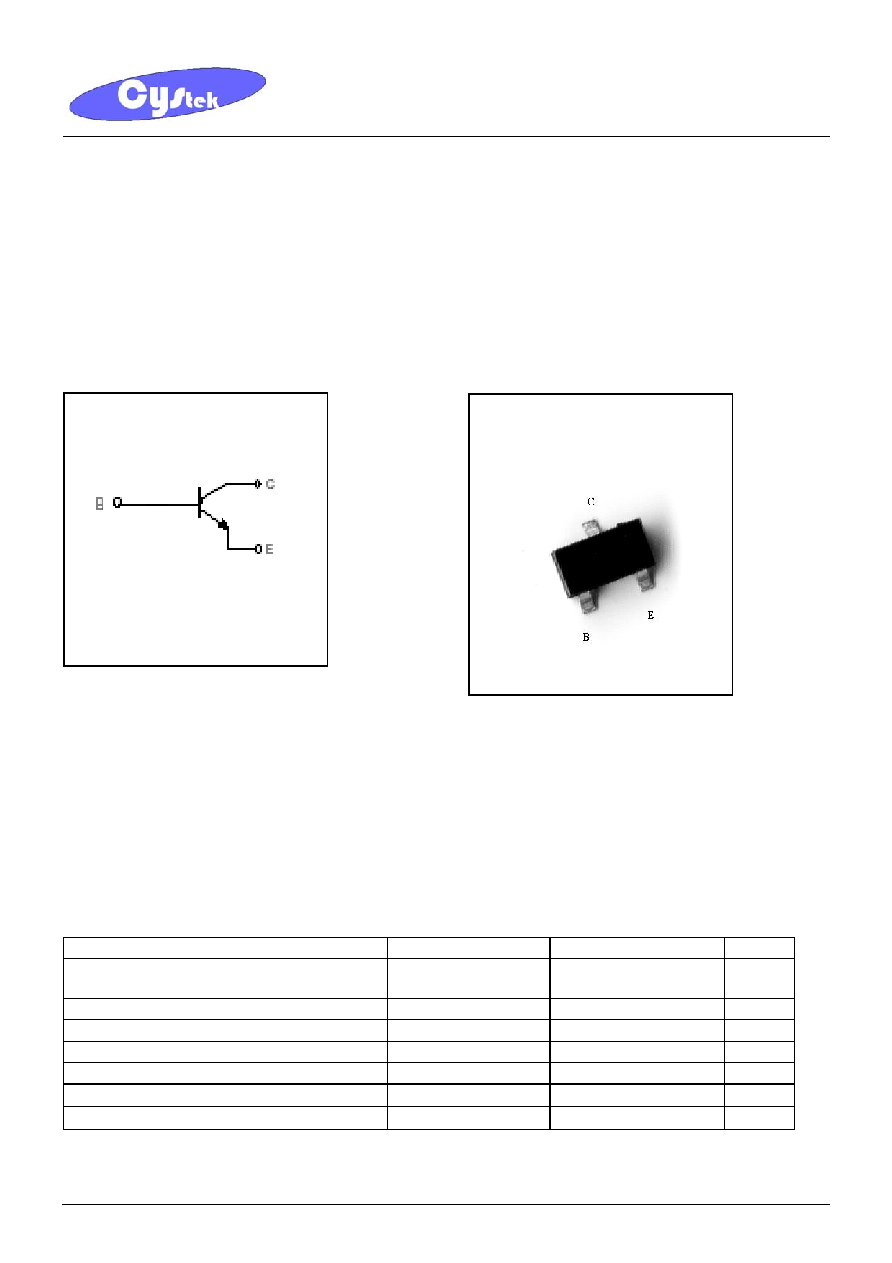
Symbol Outline
Features
∑
Low current consumption and high gain:
S
21e
≤
= 12dB ( typ. ) at V
CE
= 2 V, I
C
= 7 mA, f = 2 GHz
S
21e
≤
= 11dB ( typ. ) at V
CE
= 1 V, I
C
= 5 mA, f = 2 GHz
∑
Super mini-mold package
Applications
∑
Low noise and high gain amplifiers & Oscillator buffer amplifiers
Absolute Maximum Ratings
(T
A
=25)
Parameters Symbol
Limits
Unit
Collector-Emitter Breakdown Voltage
V
CEO
3
V
Collector-Base Breakdown Voltage
V
CBO
5
V
Emitter-Base Breakdown Voltage
V
EBO
2
V
Collector Current
I
C
10
mA
Collector Power Dissipation
Pd
30
mW
Junction Temperature
T
j
150
∞
C
Storage Temperature
T
stg
-65~+150
∞
C
SOT-323
BTC5179S3
BBase
CCollector
EEmitter
CYStech Electronics Corp.
Spec. No. : C213S3
Issued Date : 2003.04.25
Revised Date :
Page No. : 2/3
BTC5179S3
CYStek Product Specification
Electrical Characteristics
(T
A
=25
∞
C)
Parameters Conditions
Symbol
Min
Typ.
Max
Unit
Collector Cutoff Current
V
CB
=3V, I
E
=0 I
CBO
- - 100
nA
Emitter Cutoff Current
V
EB
=1V I
EBO
- - 100
nA
DC Current Gain
V
CE
=2V, I
C
=7mA
(Note 1)
h
FE
70 - 140 -
V
CE
=2V, I
C
=7mA, f =2GHz
-
12
15.5 GHz
Cutoff Frequency
V
CE
=1V, I
C
=5mA, f =2GHz
f
T
- 10 13
GHz
V
CE
=2V, I
C
=3mA, f =2GHz
-
1.5
2.0
dB
Noise Figure
V
CE
=1V, I
C
=3mA, f =2GHz
NF
- 1.5 2.0 dB
V
CE
=2V, I
C
=7mA, f =2GHz
10
12
-
dB
Insertion Gain |S
21e
|
2
in 50 system
V
CE
=1V, I
C
=5mA, f =2GHz
|S
21e
|
2
8.5 11 - dB
Output Capacitance
V
CB
=2V, IE=0, f = 1MHz
Cob
-
0.7
1.0
pF
Note 1: Pulse test: Pulse width 380µs, duty cycle 2%.
CYStech Electronics Corp.
Spec. No. : C213S3
Issued Date : 2003.04.25
Revised Date :
Page No. : 3/3
BTC5179S3
CYStek Product Specification
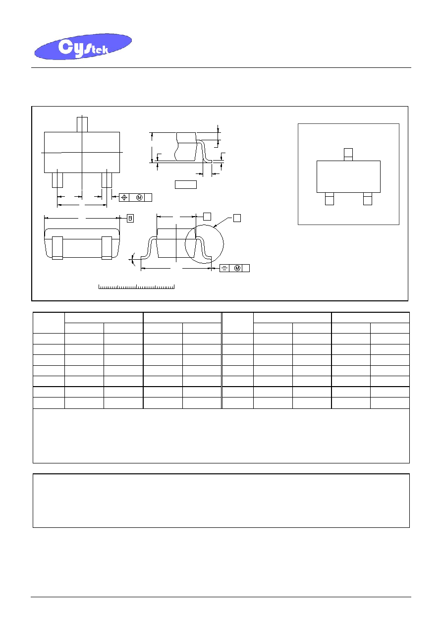
SOT-323 Dimension
*: Typical
Inches Millimeters
Inches Millimeters
DIM
Min. Max. Min. Max.
DIM
Min. Max. Min. Max.
A
0.0315
0.0433
0.80
1.10
e1
0.0256 - 0.65 -
A1 0.0000 0.0039 0.00 0.10 He 0.0787 0.0886 2.00 2.25
bp 0.0118 0.0157 0.30 0.40 Lp 0.0059
0.0177 0.15 0.45
C 0.0039
0.0098 0.10 0.25 Q 0.0051 0.0091 0.13 0.23
D 0.0709
0.0866 1.80 2.20 v 0.0079 -
0.2
-
E 0.0453
0.0531 1.15 1.35 w 0.0079 -
0.2
-
e 0.0512 -
1.3
-
- -
10
∞
0
∞
Notes:
1.Controlling dimension: millimeters.
2.Maximum lead thickness includes lead finish thickness, and minimum lead thickness is the minimum thickness of base material.
3.If there is any question with packing specification or packing method, please contact your local CYStek sales office.
Material:
∑
Lead: 42 Alloy ; solder plating
∑
Mold Compound: Epoxy resin family, flammability solid burning class: UL94V-0
Important Notice:
∑
All rights are reserved. Reproduction in whole or in part is prohibited without the prior written approval of CYStek.
∑
CYStek reserves the right to make changes to its products without notice.
∑
CYStek semiconductor products are not warranted to be suitable for use in Life-Support Applications, or systems.
∑
CYStek assumes no liability for any consequence of customer product design, infringement of patents, or application assistance.
He
E
A
A1
Q
Lp
e1
e
bp
1
2
3
D
W
B
v
A
Z
detail Z
A
C
0
1
2
scale
mm
Style: Pin 1.Base 2.Emitter 3.Collector
3-Lead SOT-323 Pastic
Surface Mounted Package
CYStek Package Code: S3
Marking:
TE
T1