CYStech Electronics Corp.
Spec. No. : C227N3
Issued Date : 2003.06.11
Revised Date :
Page No. : 1/4
BTN2222AN3
CYStek Product Specification
General Purpose NPN Epitaxial Planar Transistor
BTN2222AN3
Description
∑
The BTN2222AN3 is designed for general purpose amplifier applications. It is housed in the
SOT-23/SC-59 package which is designed for low power surface mount applications.
∑
Low V
CE(sat)
∑
Low leakage current
∑
High cutoff frequency
∑
Complementary to BTP2907AN3
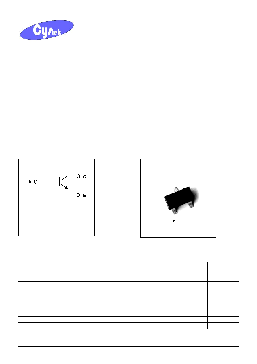
Symbol Outline
Absolute Maximum Ratings
(Ta=25
∞
C)
Parameter Symbol
Limits
Unit
Collector-Base Voltage
V
CBO
75 V
Collector-Emitter Voltage
V
CEO
40 V
Emitter-Base Voltage
V
EBO
6 V
Collector Current
I
C
600 mA
Power Dissipation @Ta=25
Derate above 25
Pd
225
(Note 1)
1.8
mW
mW/
Thermal Resistance, Junction to
Ambient
R
JA
556 /W
Junction Temperature
Tj
150
∞
C
Storage Temperature
Tstg
-55~+150
∞
C
Note 1: when mounted on a FR-5 board with area measuring 1.0◊ 0.75◊ 0.062 in.
SOT-23
BTN2222AN3
BBase
CCollector
EEmitter
CYStech Electronics Corp.
Spec. No. : C227N3
Issued Date : 2003.06.11
Revised Date :
Page No. : 2/4
BTN2222AN3
CYStek Product Specification
Characteristics
(Ta=25
∞
C)
Symbol Min. Typ. Max. Unit
Test
Conditions
BV
CBO
75 -
- V
I
C
=10µA
BV
CEO
40 -
- V
I
C
=1mA
BV
EBO
6 - - V
I
E
=10µA
I
CBO
- - 10
nA
V
CB
=60V
I
CEX
- - 10
nA
V
CE
=60V,V
EB(off)
=3V
I
EBO
- - 100
nA
V
EB
=3V
*V
CE(sat)
1 -
- 0.3 V I
C
=150mA, I
B
=15mA
*V
CE(sat)
2 -
- 1.0 V I
C
=500mA, I
B
=50mA
*V
BE(sat)
1 -
- 1.2 V I
C
=150mA, I
B
=15mA
*V
BE(sat)
2 -
- 2.0 V I
C
=500mA, I
B
=50mA
h
FE
1
35 - - -
V
CE
=10V, I
C
=0.1mA
h
FE
2
50 - - -
V
CE
=10V, I
C
=1mA
h
FE
3
75 - - -
V
CE
=10V, I
C
=10mA
*h
FE
4 100 - 300 -
V
CE
=10V, I
C
=150mA
*h
FE
5
40 - - -
V
CE
=10V, I
C
=500mA
f
T
300 - - MHz
V
CE
=20V, I
C
=20mA, f=100MHz
Cob - - 8 pF
V
CB
=10V, I
E
=0A,f=1MHz
*Pulse Test: Pulse Width
380µs, Duty Cycle
2%

CYStech Electronics Corp.
Spec. No. : C227N3
Issued Date : 2003.06.11
Revised Date :
Page No. : 3/4
BTN2222AN3
CYStek Product Specification
Characteristic Curves
Current Gain vs Collector Current
10
100
1000
0.1
1
10
100
1000
Collector Current---IC(mA)
Current Gain---
HFE
VCE=1V
V C E = 1 0 V
Saturation Voltage vs Collector Current
10
100
1000
0.1
1
10
100
1000
Collector Current---IC(mA)
Saturation Voltage---(mV)
VCE(SAT)@IC=10IB
Saturation Voltage vs Collector Current
10
100
1000
1
10
100
1000
Collector Current---IC(mA)
Saturation Voltage---(mV)
VCE(SAT)@IC=38IB
Saturation Voltage vs Collector Current
100
1000
10000
0.1
1
10
100
1000
Collector Current---IC(mA)
Saturation Voltage---(mV)
VBE(SAT)@IC=10IB
Cutoff Frequency vs Collector Current
100
1000
1
10
100
Collector Current---IC(mA)
Cutoff Frequency---fT(MHz)
V C E = 2 0 V
Power Derating Curve
0
50
100
150
200
250
0
50
100
150
200
Ambient Temperature---TA()
Power Dissipation---PD(mW
)
CYStech Electronics Corp.
Spec. No. : C227N3
Issued Date : 2003.06.11
Revised Date :
Page No. : 4/44
BTN2222AN3
CYStek Product Specification
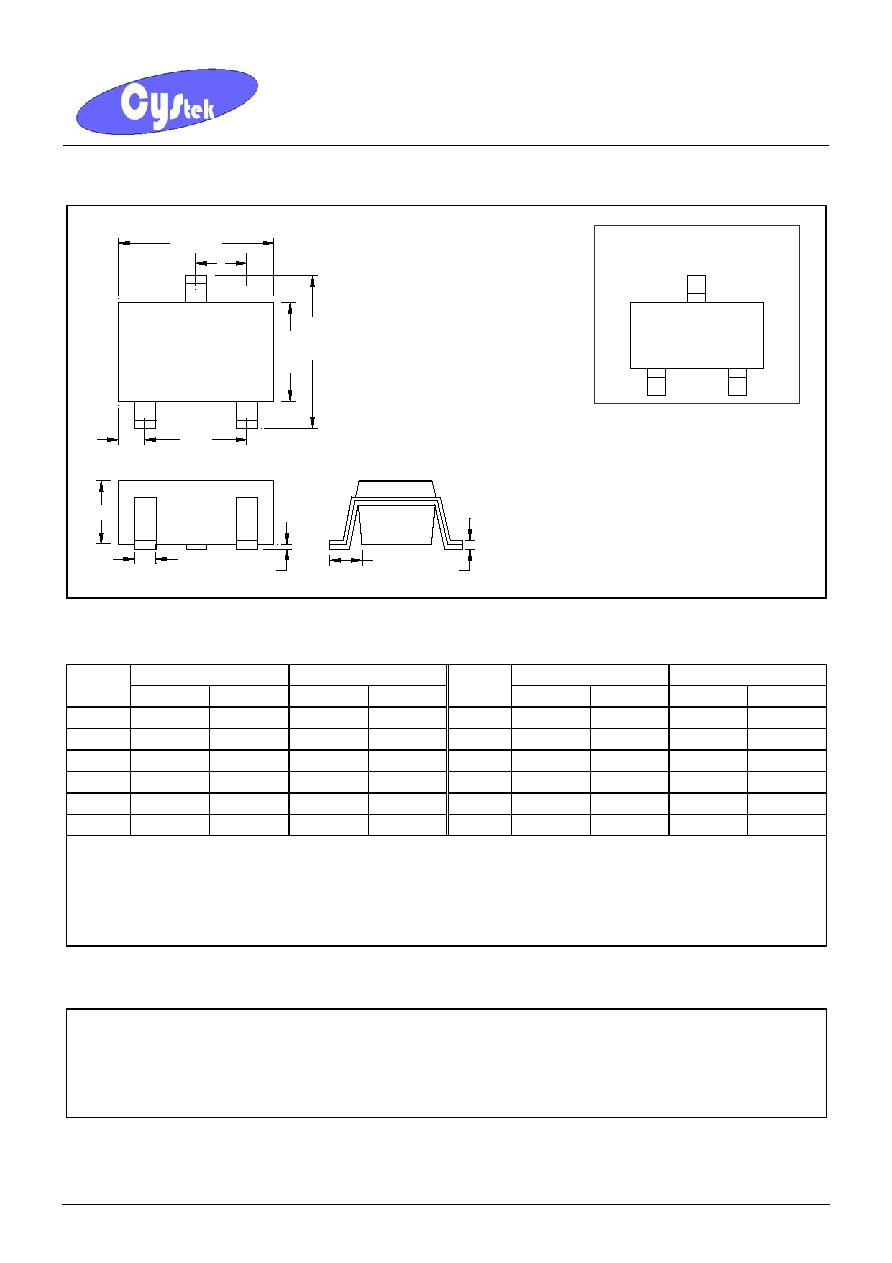
SOT-23 Dimension
*: Typical
Inches Millimeters
Inches Millimeters
DIM
Min. Max. Min. Max.
DIM
Min. Max. Min. Max.
A 0.1102
0.1204 2.80 3.04 J 0.0034
0.0070
0.085 0.177
B 0.0472
0.0630 1.20 1.60 K 0.0128 0.0266 0.32 0.67
C 0.0335
0.0512 0.89 1.30 L 0.0335 0.0453 0.85 1.15
D 0.0118
0.0197 0.30 0.50 S 0.0830
0.1083 2.10 2.75
G 0.0669
0.0910 1.70 2.30 V 0.0098 0.0256 0.25 0.65
H
0.0005
0.0040
0.013
0.10
Notes:
1.Controlling dimension: millimeters.
2.Maximum lead thickness includes lead finish thickness, and minimum lead thickness is the minimum thickness of base material.
3.If there is any question with packing specification or packing method, please contact your local CYStek sales office.
Material:
∑
Lead: 42 Alloy ; solder plating
∑
Mold Compound: Epoxy resin family, flammability solid burning class: UL94V-0
Important Notice:
∑
All rights are reserved. Reproduction in whole or in part is prohibited without the prior written approval of CYStek.
∑
CYStek reserves the right to make changes to its products without notice.
∑
CYStek semiconductor products are not warranted to be suitable for use in Life-Support Applications, or systems.
∑
CYStek assumes no liability for any consequence of customer product design, infringement of patents, or application assistance.
H
J
K
D
A
L
G
V
C
B
3
2
1
S
Style: Pin 1.Base 2.Emitter 3.Collector
Marking:
TE
3-Lead SOT-23 Plastic
Surface Mounted Package
CYStek Package Code: N3
1P