 | –≠–ª–µ–∫—Ç—Ä–æ–Ω–Ω—ã–π –∫–æ–º–ø–æ–Ω–µ–Ω—Ç: DAN217S3 | –°–∫–∞—á–∞—Ç—å:  PDF PDF  ZIP ZIP |

CYStech Electronics Corp.
Spec. No. : C303S3C
Issued Date : 2003.10.07
Revised Date : . .
Page No. : 1/4
DAN217S3
CYStek Product Specification
DAN217S3
HIGH-SPEED SWITCHING DIODE
Description
The DAN217S3 consists of two diodes in a plastic surface mount package. The diodes are
connected in series and the unit is designed for high-speed switching application in hybrid thick
and thin-film circuits.
Features
∑
Small SMD Package (SOT-323)
∑
Ultra-high Speed
∑
Low Forward Voltage
∑
Fast Reverse Recovery Time
Equivalent Circuit Outline
3
1
2
Absolute Maximum Ratings
∑
Maximum Temperatures
Storage Temperature............................................................................................ -65 ~ +150
∞
C
Junction Temperature .................................................................................................... +150
∞
C
∑
Maximum Power Dissipation
Total Power Dissipation (Ta=25
∞
C) ................................................................................ 200 mW
∑
Maximum Voltages and Currents (Ta=25
∞
C)
Reverse Voltage .................................................................................................................. 70 V
Repetitive Reverse Voltage ................................................................................................. 70 V
Forward Current ............................................................................................................. 150 mA
Repetitive Forward Current ............................................................................................ 500 mA
Forward Surge Current (1ms)....................................................................................... 1000 mA
1. Anode 1
2. Cathode 2
3. Cathode 1 / Anode 2
K1, A2
A1
K2
Sot-323
CYStech Electronics Corp.
Spec. No. : C303S3C
Issued Date : 2003.10.07
Revised Date : . .
Page No. : 2/4
DAN217S3
CYStek Product Specification
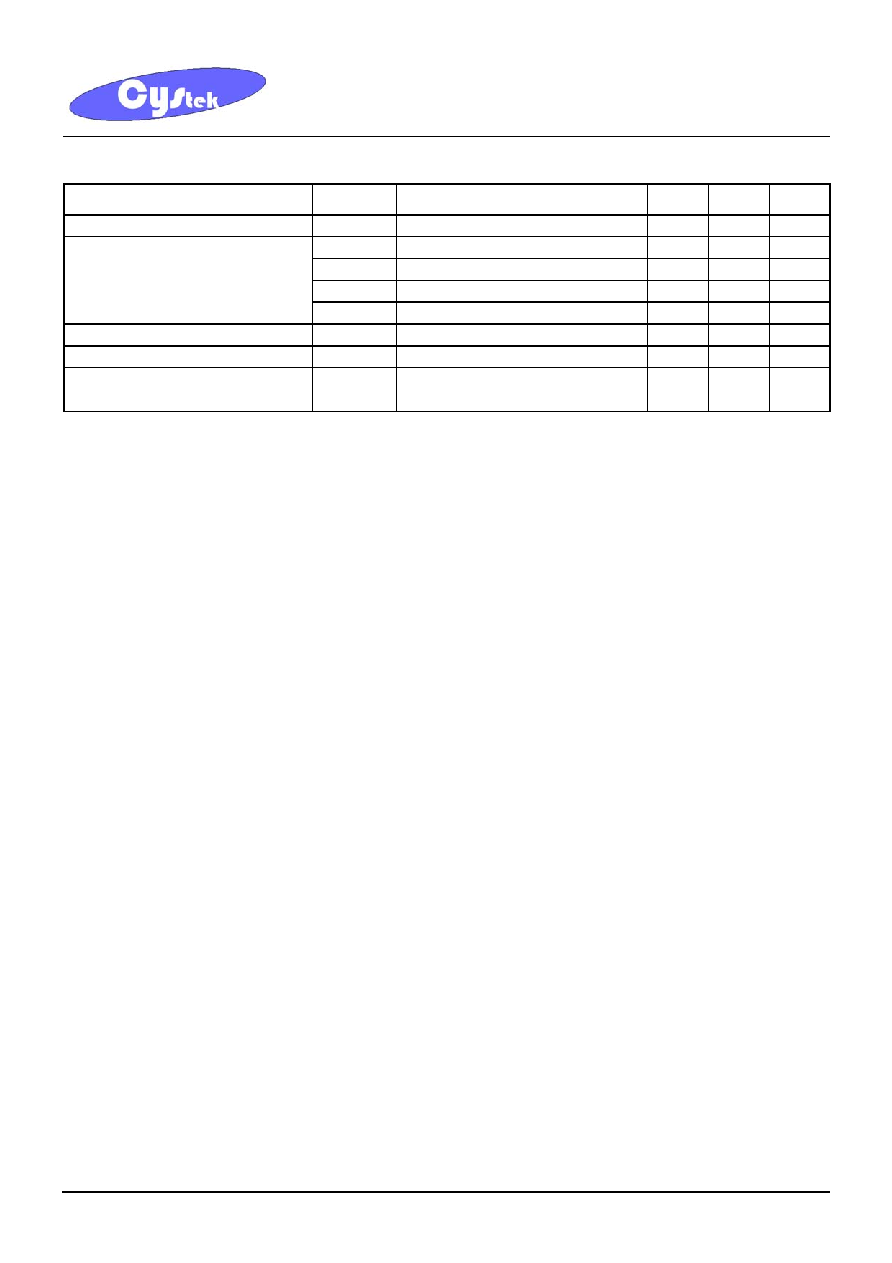
Characteristics
(Ta=25
∞
C)
Characteristic Symbol Condition
Min
Max
Unit
Reverse Breakdown Voltage
V
(BR)
I
R
=100µA 70
-
V
V
F
(1) I
F
=1mA -
715
mV
V
F
(2) I
F
=10mA -
855
mV
V
F
(3) I
F
=50mA -
1000
mV
Forward Voltage
V
F
(4) I
F
=150mA -
1250
mV
Reverse Current
I
R
V
R
=70 -
2.5
µA
Total Capacitance
C
T
V
R
=0, f=1MHz
-
1.5
pF
Reverse Recovery Time
t
rr
I
F
=I
R
=10mA, R
L
=100
measured at I
R
=1mA
- 6 ns

CYStech Electronics Corp.
Spec. No. : C303S3C
Issued Date : 2003.10.07
Revised Date : . .
Page No. : 3/4
DAN217S3
CYStek Product Specification
Characteristic Curves
Forward Biased Voltage & Forward Current
0
150
300
450
0
500
1000
1500
2000
Forward Biased Voltage-VF (mV)
Cu
r
r
e
n
t
-
I
F
(m
A
)
Capacitance & Reverse-Biased Voltage
0.1
1
0.1
1
10
100
Reverse Biased Voltage-V
R
(V)
C
a
p
a
c
i
ta
n
c
e
-
C
d
(p
F
)

CYStech Electronics Corp.
Spec. No. : C303S3C
Issued Date : 2003.10.07
Revised Date : . .
Page No. : 4/4
DAN217S3
CYStek Product Specification
SOT-323 Dimension
*: Typical
Inches Millimeters
Inches Millimeters
DIM
Min. Max. Min. Max.
DIM
Min. Max. Min. Max.
A
0.0315
0.0433
0.80
1.10
e1
0.0256 - 0.65 -
A1 0.0000 0.0039 0.00 0.10 He 0.0787 0.0886 2.00 2.25
bp 0.0118 0.0157 0.30 0.40 Lp 0.0059
0.0177 0.15 0.45
C 0.0039
0.0098 0.10 0.25 Q 0.0051 0.0091 0.13 0.23
D 0.0709
0.0866 1.80 2.20 v 0.0079 -
0.2
-
E 0.0453
0.0531 1.15 1.35 w 0.0079 -
0.2
-
e 0.0512 -
1.3
-
- -
10
∞
0
∞
Notes:
1.Controlling dimension: millimeters.
2.Maximum lead thickness includes lead finish thickness, and minimum lead thickness is the minimum thickness of base material.
3.If there is any question with packing specification or packing method, please contact your local CYStek sales office.
Material:
∑
Lead: 42 Alloy ; solder plating
∑
Mold Compound: Epoxy resin family, flammability solid burning class: UL94V-0
Important Notice:
∑
All rights are reserved. Reproduction in whole or in part is prohibited without the prior written approval of CYStek.
∑
CYStek reserves the right to make changes to its products without notice.
∑
CYStek semiconductor products are not warranted to be suitable for use in Life-Support Applications, or systems.
∑
CYStek assumes no liability for any consequence of customer product design, infringement of patents, or application assistance.
He
E
A
A1
Q
Lp
e1
e
bp
1
2
3
D
W
B
v
A
Z
detail Z
A
C
0
1
2
scale
mm
Style : Pin 1. A1 2.K2 3. K1, A2
3-Lead SOT-323 Plastic
Surface Mounted Package
CYStek Package Code: S3
Marking:
TE
KJG