CYStech Electronics Corp.
Spec. No. : C380N3
Issued Date : 2005.04.15
Revised Date :2005.06.24
Page No. : 1/6
DTD143TN3
CYStek Product Specification
NPN Digital Transistors (Built-in Resistors)
DTD143TN3
Features
∑
Built-in bias resistors enable the configuration of an inverter circuit without connecting external input
resistors (see equivalent circuit).
∑
The bias resistors consist of thin-film resistors with complete isolation to allow negative biasing of the
input. They also have the advantage of almost completely eliminating parasitic effects.
∑
Only the on/off conditions need to be set for operation, making device design easy.
∑
Complements the DTB143TN3
∑
Pb-free package
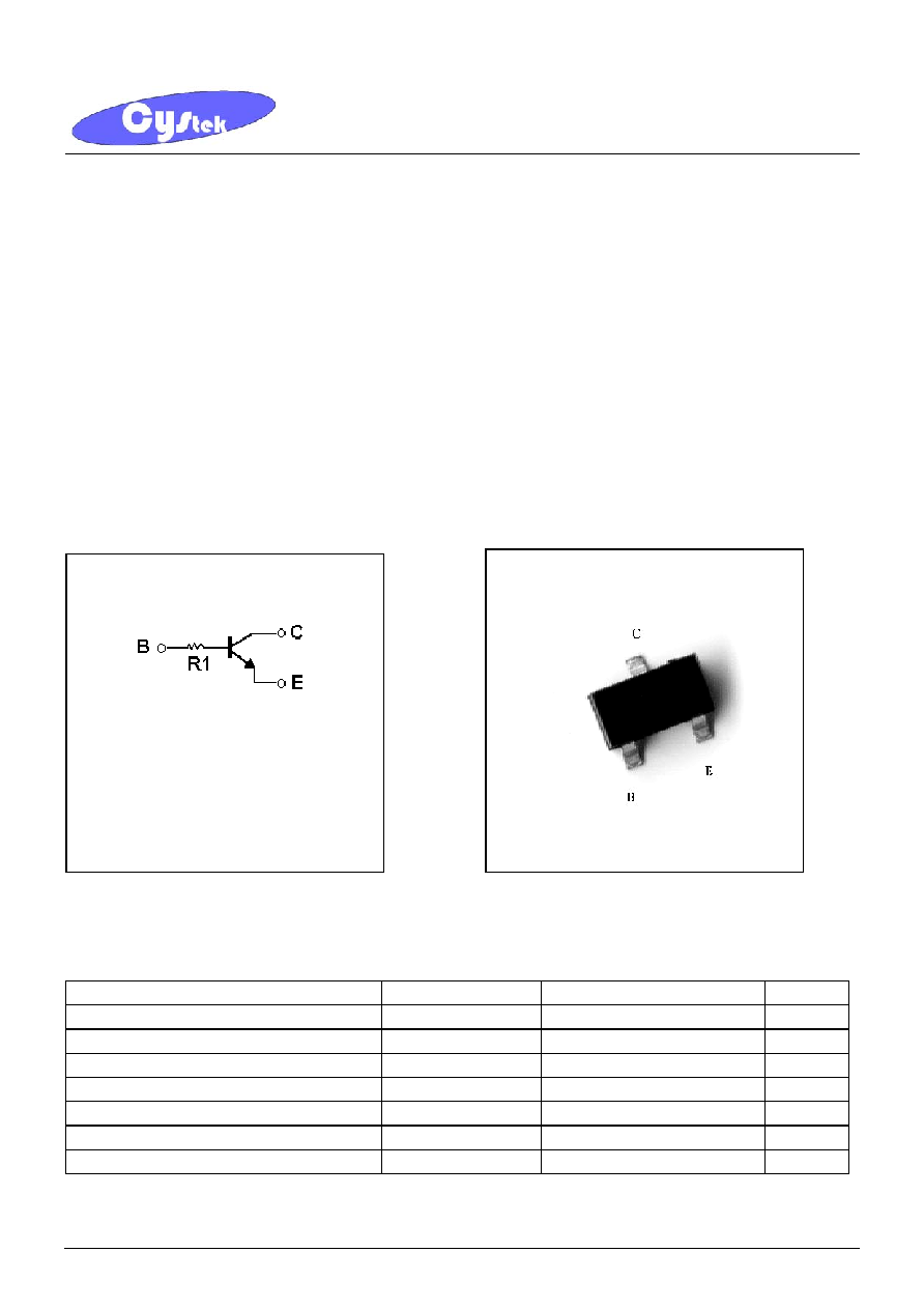
Equivalent Circuit Outline
Absolute Maximum Ratings
(Ta=25)
Parameter Symbol
Limits
Unit
Collector-Base Voltage
V
CBO
50
V
Collector-Emitter Voltage
V
CEO
40
V
Emitter-Base Voltage
V
EBO
5
V
Collector Current
I
C
600
mA
Power Dissipation
Pd
200
mW
Junction Temperature
Tj
150
∞
C
Storage Temperature
Tstg
-55 ~ +150
∞
C
SOT-23
DTD143TN3
R1=4.7k
,
B : Base
C : Collector
E : Emitter
CYStech Electronics Corp.
Spec. No. : C380N3
Issued Date : 2005.04.15
Revised Date :2005.06.24
Page No. : 2/6
DTD143TN3
CYStek Product Specification
Characteristics
(Ta=25)
Parameter Symbol
Min. Typ. Max. Unit
Test
Conditions
Collector-Base Breakdown Voltage
V
CBO
50 -
- V
I
C
=50µA
Collector-Emitter Breakdown
Voltage
V
CEO
40 -
- V
I
C
=1mA
Emitter-Base Breakdown Voltage
V
EBO
5 -
- V
I
E
=50µA
Collector-Base Cutoff Current
I
CBO
- -
0.5
µA
V
CB
=50V
Emitter-Base Cutoff Current
I
EBO
- -
0.5
µA
V
EB
=4V
Collector-Emitter Saturation
Voltage
V
CE(sat)
- 40 60
mV I
C
=50mA, I
B
=2.5mA
DC Current Gain
h
FE
100
- 600
-
V
CE
=5V, I
C
=50mA
Input Resistance
R
1
3.29
4.7
6.11
k
-
Transition Frequency
f
T
-
200
-
MHz V
CE
=10V, I
C
=50mA, f=100MHz *
*
Transition frequency of the device
Ordering Information
Device Package
Shipping
Marking
DTD143TN3
SOT-23
(Pb-free)
3000 pcs / Tape & Reel
F03

CYStech Electronics Corp.
Spec. No. : C380N3
Issued Date : 2005.04.15
Revised Date :2005.06.24
Page No. : 3/6
DTD143TN3
CYStek Product Specification
Characteristic Curves
Current Gain vs Collector Current
100
1000
0.1
1
10
100
1000
Collector Current---IC(mA)
Current Gain---
HFE
VCE=5V
Saturation Voltage vs Collector Current
10
100
1000
0.1
1
10
100
1000
Collector Current --- IC(mA)
Saturation Voltage---(mV)
VCESAT@IC=20IB
Power Derating Curve
0
50
100
150
200
250
0
50
100
150
200
Ambient Temperature --- Ta( )
Power Dissipation---PD(mW)

CYStech Electronics Corp.
Spec. No. : C380N3
Issued Date : 2005.04.15
Revised Date :2005.06.24
Page No. : 4/6
DTD143TN3
CYStek Product Specification
Product Designation
DT X X X X X XX
(1) (2) (3) (4) (5) (6) (7)
(1) Indicates that transistor is digital (6) Indicates resistance ratio R
1
/R
2
E R
1
/R
2
=1/1
(2) Indicates polarity X R
1
/R
2
=2/1
A, B PNP Y R
1
/R
2
=5/1
C, D NPN Z R
1
/R
2
=10/1
J R
1
/R
2
=20/1
(3) Indicates device specification WR
1
/R
2
=1/2
U R
1
/R
2
=1/5
(4) Indicates the basis of the R
1
resistance value V R
1
/R
2
=1/10
11.0 T R
1
only
22.2 G T
2
only
33.3
44.7
66.8 (7) Indicates package shape
N3SOT-23
(5) Indicates power-of-ten of R
1
value A3TO-92
310
3
410
4
The value of R1 is indicates by combining (4) and (5)
242.2◊10
4
=22k
434.7◊10
3
=22k
CYStech Electronics Corp.
Spec. No. : C380N3
Issued Date : 2005.04.15
Revised Date :2005.06.24
Page No. : 5/6
DTD143TN3
CYStek Product Specification
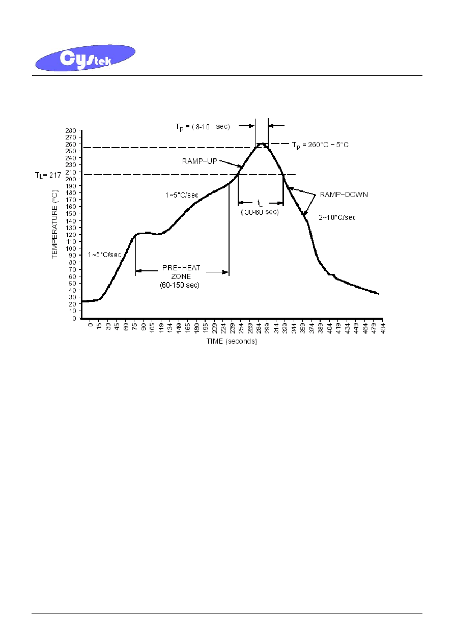
Recommended IR reflow profile