 | –≠–ª–µ–∫—Ç—Ä–æ–Ω–Ω—ã–π –∫–æ–º–ø–æ–Ω–µ–Ω—Ç: DTC114EA3 | –°–∫–∞—á–∞—Ç—å:  PDF PDF  ZIP ZIP |
CYStech Electronics Corp.
Spec. No. : C252A3
Issued Date : 2003.09.29
Revised Date :
Page No. : 1/6
DTA114EA3
CYStek Product Specification
PNP Digital Transistors (Built-in Resistors
)
DTA114EA3
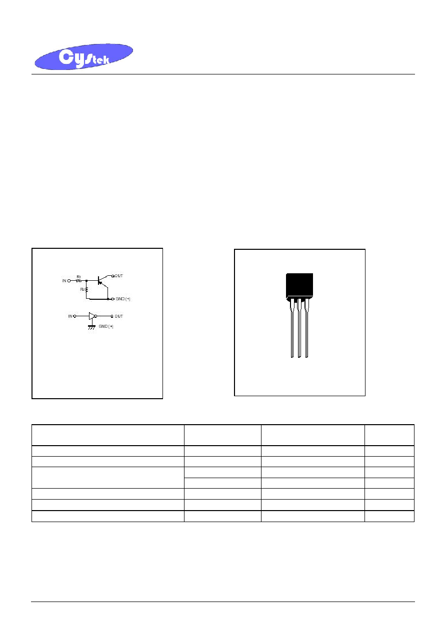
Features
∑
Built-in bias resistors enable the configuration of an inverter circuit without connecting external input
resistors (see equivalent circuit).
∑
The bias resistors consist of thin-film resistors with complete isolation to allow positive biasing of the
input. They also have the advantage of almost completely eliminating parasitic effects.
∑
Only the on/off conditions need to be set for operation, making device design easy.
∑
Complements the DTC114EA3
Equivalent Circuit Outline
Absolute Maximum Ratings
(Ta=25
∞
C)
Parameter Symbol
Limits
Unit
Supply Voltage
V
CC
-50
V
Input Voltage
V
IN
-40~+10
V
I
O
-50
mA
Output Current
I
O(max)
-100
mA
Power Dissipation
Pd
400
mW
Junction Temperature
Tj
150
∞
C
Storage Temperature
Tstg
-55~+150
∞
C
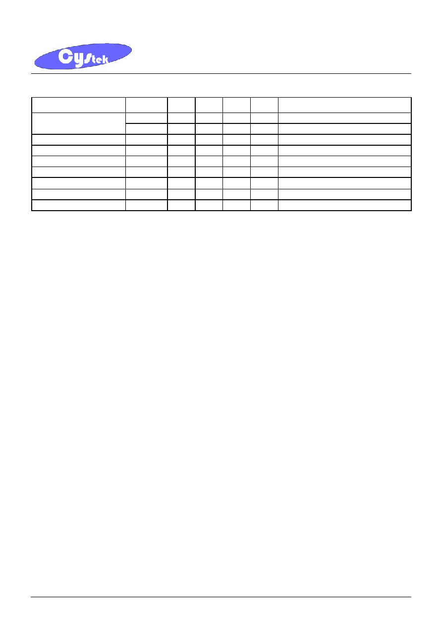
TO-92
DTA114EA3
R1=10k
, R2=10 k
IN(B) : Base
OUT(C) : Collector
GND(E) : Emitter
G O I
CYStech Electronics Corp.
Spec. No. : C252A3
Issued Date : 2003.09.29
Revised Date :
Page No. : 2/6
DTA114EA3
CYStek Product Specification
Electrical Characteristics
(Ta=25
∞
C)
Parameter Symbol
Min.
Typ.
Max.
Unit Test
Conditions
V
I(off)
- - -0.5
V
V
CC
=-5V, I
O
=-100µA
Input Voltage
V
I(on)
-3 - - V
V
O
=-0.3V, Io=-10mA
Output Voltage
V
O(on)
- - -0.3
V
I
O
/I
I
=-10mA/-0.5mA
Input Current
I
I
-
-
-0.88
mA
V
I
=-5V
Output Current
I
O(off)
- -
-0.5
µA
V
CC
=-50V, V
I
=0V
DC Current Gain
G
I
30 - - -
V
O
=-5V, I
O
=-5mA
Input Resistance
R
1
7
10
13
k
-
Resistance Ratio
R
2
/R
1
0.8 1 1.2 - -
Transition Frequency
f
T
-
250
-
MHz
V
CE
=-10V, I
C
=-5mA, f=100MHz *
* Transition frequency of the device
CYStech Electronics Corp.
Spec. No. : C252A3
Issued Date : 2003.09.29
Revised Date :
Page No. : 3/6
DTA114EA3
CYStek Product Specification
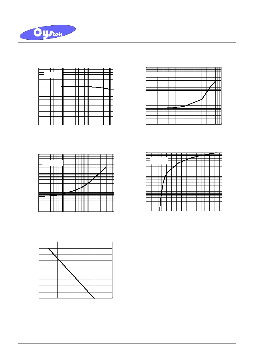
Characteristic Curves
Current Gain vs Output Current
10
100
1000
0.1
1
10
100
Output Current---I
O
(mA)
Current Gain---G
I
Vo = 5V
Output Voltage vs Output Current
0.01
0.1
1
10
1
10
100
Output Current---I
O
(mA)
Output Voltage---V
O(ON)
(V)
Io / Ii = 20
Input Voltage vs Output Current(ON characteristics)
0.1
1
10
100
0.1
1
10
100
Output Current---I
O
(mA)
Input Voltage---V
I(ON)
(V)
Vo = 0.3V
Output Current vs Input Voltage(OFF characteristics)
0.01
0.1
1
10
0
0.5
1
1.5
2
2.5
3
Input Voltage---V
I(OFF)
(V)
Output Current---I
O
(mA)
V
CC
= 5 V
Power Derating Curve
0
50
100
150
200
250
300
350
400
450
0
50
100
150
200
Ambient Temperature---T
A
()
Power Dissipation---P
D
(mW)
CYStech Electronics Corp.
Spec. No. : C252A3
Issued Date : 2003.09.29
Revised Date :
Page No. : 4/6
DTA114EA3
CYStek Product Specification
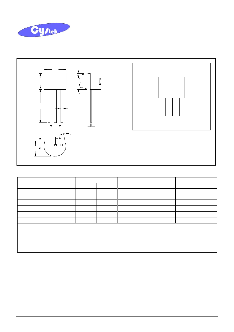
TO-92 Dimension
*: Typical
Inches Millimeters
Inches Millimeters
DIM
Min. Max. Min. Max.
DIM
Min. Max. Min. Max.
A 0.1704
0.1902 4.33 4.83 G 0.0142 0.0220 0.36 0.56
B 0.1704
0.1902 4.33 4.83 H
-
*
0.1000 -
*
2.54
C 0.5000 - 12.70 -
I
-
*
0.0500 -
*
1.27
D 0.0142
0.0220 0.36 0.56
1
-
*
5
∞
-
*
5
∞
E -
*
0.0500 -
*
1.27
2
-
*
2
∞
-
*
2
∞
F 0.1323
0.1480 3.36 3.76
3
-
*
2
∞
-
*
2
∞
Notes:
1.Controlling dimension: millimeters.
2.Maximum lead thickness includes lead finish thickness, and minimum lead thickness is the minimum thickness of base material.
3.If there is any question with packing specification or packing method, please contact your local CYStek sales office.
Material:
∑
Lead: 42 Alloy ; solder plating
∑
Mold Compound: Epoxy resin family, flammability solid burning class: UL94V-0
DTA114E
Marking:
3
1
A
D
B
C
I
1
E
F
2
3
G
H
2
Style : Pin 1.GND(Emitter) 2.OUT(Collector)
3.IN(Base)
3-Lead TO-92 Plastic Package
CYStek Package Code: A3

CYStech Electronics Corp.
Spec. No. : C252A3
Issued Date : 2003.09.29
Revised Date :
Page No. : 5/6
DTA114EA3
CYStek Product Specification
TO-92 Taping Outline
Millimeters
DIM Item
Min. Max.
A
Component body height
4.33
4.83
D
Tape Feed Diameter
3.80
4.20
D1 Lead
Diameter
0.36
0.53
D2
Component Body Diameter
4.33
4.83
F1,F2
Component Lead Pitch
2.40
2.90
F1,F2 F1-F2
-
±
0.3
H
Height Of Seating Plane
15.50
16.50
H1
Feed Hole Location
8.50
9.50
H2
Front To Rear Deflection
-
1
H2A
Deflection Left Or Right
-
1
H3 Component
Height
-
27
H4
Feed Hole To Bottom Of Component
-
21
L
Lead Length After Component Removal
-
11
L1
Lead Wire Enclosure
2.50
-
P
Feed Hole Pitch
12.50
12.90
P1
Center Of Seating Plane Location
5.95
6.75
P2
4 Feed Hole Pitch
50.30
51.30
T
Over All Tape Thickness
-
0.55
T1
Total Taped Package Thickness
-
1.42
T2
Carrier Tape Thickness
0.36
0.68
W Tape
Width
17.50
19.00
W1
Adhesive Tape Width
5.00
7.00
-
20 pcs Pitch
253
255
H2A
H2A
H2
H2
D2
A
H
W
W1
H3
H4
H1
L1
L
P2
P
P1
F1F2
D1
D
T2
T
T1